
© 1999 Fairchild Semiconductor Corporation
DS500297
www.fairchildsemi.com
August 1999
Revised October 1999
7
4
AC
T1
6373
1
6
-Bi
t
T
r
anspa
rent
Lat
ch w
i
th 3-
ST
A
T
E O
u
t
put
s
74ACT16373
16-Bit Transparent Latch with 3-STATE Outputs
General Description
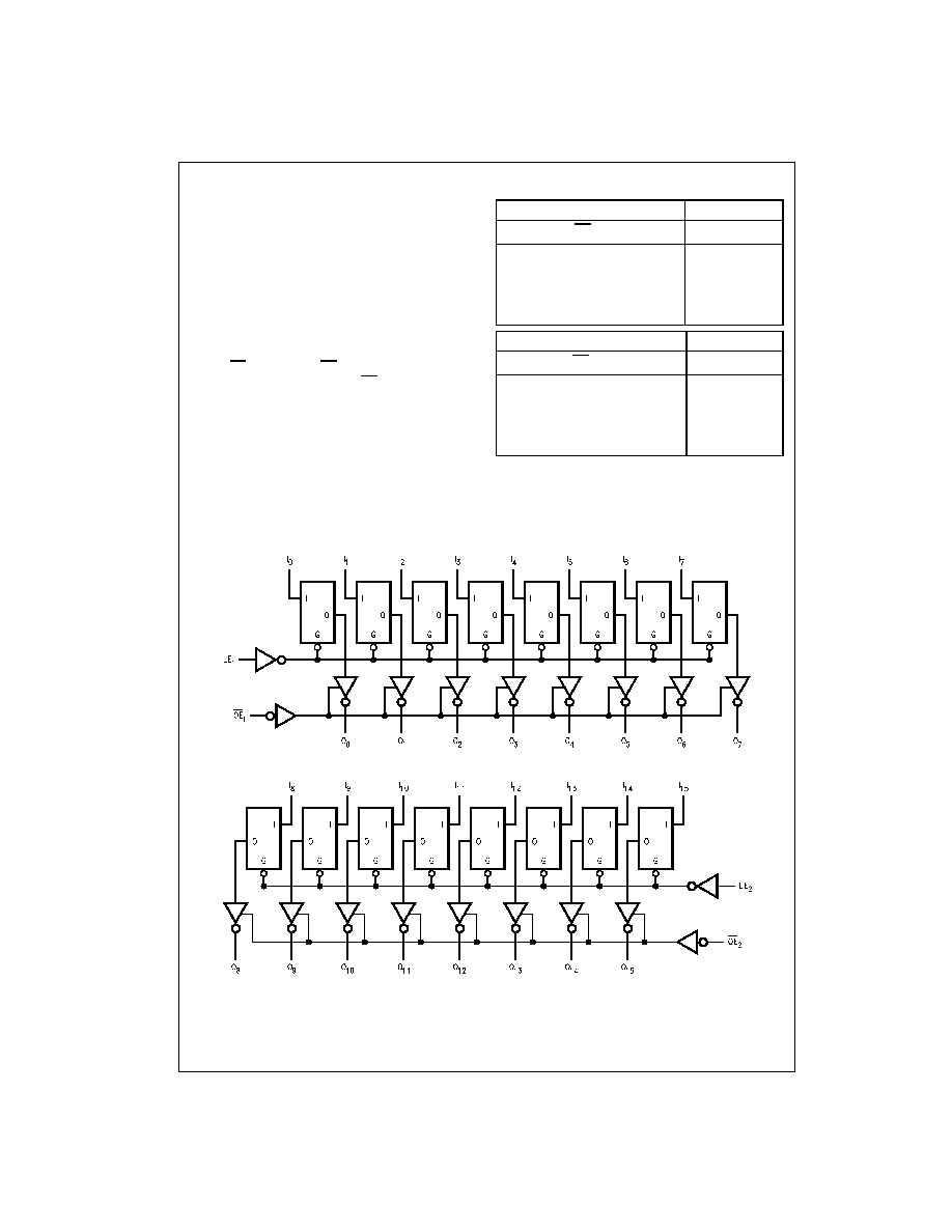
The ACT16373 contains sixteen non-inverting latches with
3-STATE outputs and is intended for bus oriented applica-
tions. The device is byte controlled. The flip-flops appear
transparent to the data when the Latch Enable (LE) is
HIGH. When LE is low, the data that meets the setup time
is latched. Data appears on the bus when the Output
Enable (OE) is LOW. When OE is HIGH, the outputs are in
high Z state.
Features
s
Separate control logic for each byte
s
16-bit version of the ACT373
s
Outputs source/sink 24 mA
s
TTL-compatible inputs
Ordering Code:
Device also available in Tape and Reel. Specify by appending suffix letter "X" to the ordering code.
Logic Symbol
Pin Descriptions
Connection Diagram
FACT
TM
is a trademark of Fairchild Semiconductor Corporation.
Order Number
Package Number
Package Description
74ACT16373MEA
MS48A
48-Lead Small Shrink Outline Package (SSOP), JEDEC MO-118, 0.300" Wide
74ACT16373MTD
MTD48
48-Lead Thin Shrink Small Outline Package (TSSOP), JEDEC MO-153, 6.1mm Wide
Pin Names
Description
OE
n
Output Enable Input (Active Low)
LE
n
Latch Enable Input
I
0
≠I
15
Inputs
O
0
≠O
15
Outputs
www.fairchildsemi.com
2
74ACT16373
Functional Description
The ACT16373 contains sixteen D-type latches with 3-
STATE standard outputs. The device is byte controlled with
each byte functioning identically, but independent of the
other. Control pins can be shorted together to obtain full
16-bit operation. The following description applies to each
byte. When the Latch Enable (LE
n
) input is HIGH, data on
the D
n
enters the latches. In this condition the latches are
transparent, i.e., a latch output will change states each time
its D input changes. When LE
n
is LOW, the latches store
information that was present on the D inputs a setup time
preceding the HIGH-to-LOW transition of LE
n
. The 3-
STATE standard outputs are controlled by the Output
Enable (OE
n
) input. When OE
n
is LOW, the standard out-
puts are in the 2-state mode. When OE
n
is HIGH, the stan-
dard outputs are in the high impedance mode but this does
not interfere with entering new data into the latches.
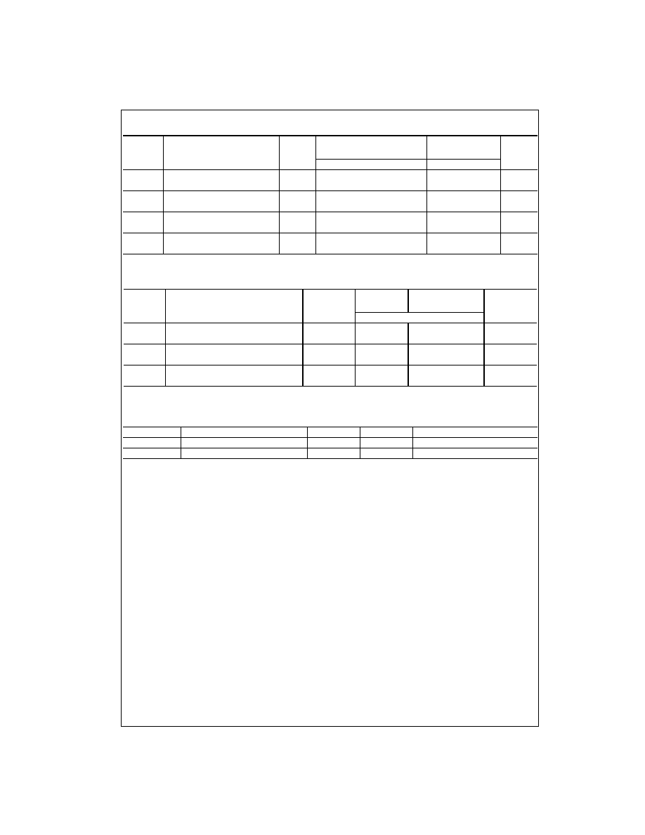
Truth Tables
H
=
HIGH Voltage Level
L
=
LOW Voltage Level
X
=
Immaterial
Z
=
High Impedance
Previous
=
previous output prior to HIGH-to-LOW transition of LE
Logic Diagrams
Inputs
Outputs
LE
1
OE
1
I
0
≠I
7
O
0
≠O
7
X
H
X
Z
H
L
L
L
H
L
H
H
L
L
X
(Previous)
Inputs
Outputs
LE
2
OE
2
I
8
≠I
15
O
8
≠O
15
X
H
X
Z
H
L
L
L
H
L
H
H
L
L
X
(Previous)
3
www.fairchildsemi.com
7
4
AC
T1
6373
Absolute Maximum Ratings
(Note 1)
Recommended Operating
Conditions
Note 1: Absolute maximum ratings are those values beyond which dam-
age to the device may occur. The databook specifications should be met,
without exception to ensure that the system design is reliable over its power
supply, temperature, and output/input loading variables. Fairchild does not
recommend operation of FACT
TM
circuits outside databook specifications.
DC Electrical Characteristics
Note 2: All outputs loaded; thresholds associated with output under test.
Note 3: Maximum test duration 2.0 ms; one output loaded at a time.
Supply Voltage (V
CC
)
-
0.5V to
+
7.0V
DC Input Diode Current (I
IK
)
V
I
=
-
0.5V
-
20 mA
V
I
=
V
CC
+
0.5V
+
20 mA
DC Output Diode Current (I
OK
)
V
O
=
-
0.5V
-
20 mA
V
O
=
V
CC
+
0.5V
+
20 mA
DC Output Voltage (V
O
)
-
0.5V to V
CC
+
0.5V
DC Output Source/Sink Current (I
O
)
+
50 mA
DC V
CC
or Ground Current
+
50 mA
per Output Pin
Junction Temperature
+
140
∞
C
Storage Temperature
-
65
∞
C to
+
150
∞
C
Supply Voltage (V
CC
)
4.5V to 5.5V
Input Voltage (V
I
)
0V to V
CC
Output Voltage (V
O
)
0V to V
CC
Operating Temperature (T
A
)
-
40
∞
C to
+
85
∞
C
Minimum Input Edge Rate (
V/
t)
125 mV/ns
V
IN
from 0.8V to 2.0V
V
CC
@ 4.5V, 5.5V
Symbol
Parameter
V
CC
T
A
=
+
25
∞
C
T
A
=
-
40
∞
C to
+
85
∞
C
Units
Conditions
(V)
Typ
Guaranteed Limits
V
IH
Minimum HIGH
4.5
1.5
2.0
2.0
V
V
OUT
=
0.1V
Input Voltage
5.5
1.5
2.0
2.0
or V
CC
-
0.1V
V
IL
Maximum LOW
4.5
1.5
0.8
0.8
V
V
OUT
=
0.1V
Input Voltage
5.5
1.5
0.8
0.8
or V
CC
-
0.1V
V
OH
Minimum HIGH
4.5
4.49
4.4
4.4
V
I
OUT
=
-
50
µ
A
Output Voltage
5.5
5.49
5.4
5.4
V
IN
=
V
IL
or V
IH
4.5
3.86
3.76
V
I
OH
=
-
24 mA
5.5
4.86
4.76
I
OH
=
-
24 mA (Note 2)
V
OL
Maximum LOW
4.5
0.001
0.1
0.1
V
I
OUT
=
50
µ
A
Output Voltage
5.5
0.001
0.1
0.1
V
IN
=
V
IL
or V
IH
4.5
0.36
0.44
V
I
OL
=
24 mA
5.5
0.36
0.44
I
OL
=
24 mA (Note 2)
I
OZ
Maximum 3-STATE
5.5
±
0.5
±
5.0
µ
A
V
I
=
V
IL
, V
IH
Leakage Current
V
O
=
V
CC
, GND
I
IN
Maximum Input
5.5
±
0.1
±
1.0
µ
A
V
I
=
V
CC
, GND
Leakage Current
I
CCT
Maximum I
CC
/Input
5.5
0.6
1.5
mA
V
I
=
V
CC
-
2.1V
I
CC
Max Quiescent Supply Current
5.5
8.0
80.0
µ
A
V
IN
=
V
CC
or GND
I
OLD
Minimum Dynamic
5.5
75
mA
V
OLD
=
1.65V Max
I
OHD
Output Current (Note 3)
-
75
mA
V
OHD
=
3.85V Min
www.fairchildsemi.com
4
74ACT16373
AC Electrical Characteristics
Note 4: Voltage Range 5.0 is 5.0V
±
0.5V.
AC Operating Requirements
Note 5: Voltage Range 5.0 is 5.0V
±
0.5V
Capacitance
V
CC
T
A
=
+
25
∞
C
T
A
=
-
40
∞
C to
+
85
∞
C
Symbol
Parameter
(V)
C
L
=
50 pF
C
L
=
50 pF
Units
(Note 4)
Min
Typ
Max
Min
Max
t
PLH
Propagation Delay
5.0
3.1
5.3
7.9
3.1
8.4
ns
t
PHL
D
n
to O
n
2.6
4.6
7.3
2.6
7.8
t
PLH
Propagation Delay
5.0
3.1
5.4
7.9
3.2
8.4
ns
t
PHL
LE to O
n
2.8
4.9
7.3
2.8
7.8
t
PZH
Output Enable
5.0
2.5
4.7
7.4
2.5
7.9
ns
t
PZL
Delay
2.7
4.8
7.5
2.7
8.0
t
PHZ
Output Disable
5.0
2.1
5.1
7.9
2.1
8.2
ns
t
PLZ
Delay
2.0
4.5
7.4
2.0
7.9
V
CC
T
A
=
+
25
∞
C
T
A
=
-
40
∞
C to
+
85
∞
C
Units
Symbol
Parameter
(V)
C
L
=
50 pF
C
L
=
50 pF
(Note 5)
Guaranteed Minimum
t
S
Setup Time, HIGH or
5.0
3.0
3.0
ns
LOW, Input to Clock
t
H
Hold time, HIGH or
5.0
1.5
1.5
ns
LOW, Input to Clock
t
W
CS Pulse Width,
5.0
4.0
4.0
ns
HIGH or LOW
Symbol
Parameter
Typ
Units
Conditions
C
IN
Input Capacitance
4.5
pF
V
CC
=
5.0V
C
PD
Power Dissipation Capacitance
30
pF
V
CC
=
5.0V
5
www.fairchildsemi.com
7
4
AC
T1
6373
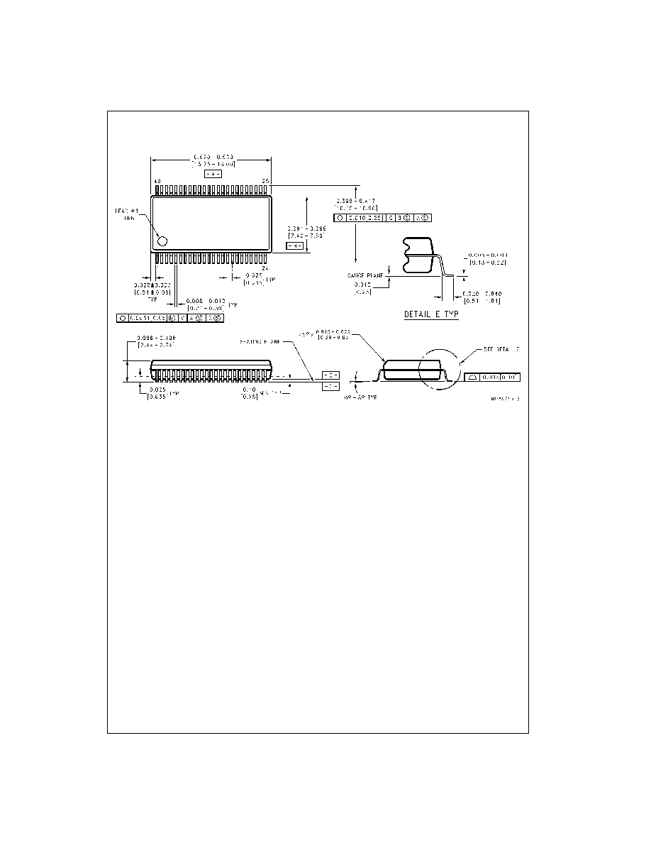
Physical Dimensions
inches (millimeters) unless otherwise noted
48-Lead Small Shrink Outline Package (SSOP), JEDEC MO-118, 0.300" Wide
Package Number MS48A