© 2000 Fairchild Semiconductor Corporation
DS009932
www.fairchildsemi.com
November 1988
Revised February 2000
74
A
C
16
3
∑ 74ACT163 Synchronous
Pre
sett
able
Bi
nary Counter
74AC163 ∑ 74ACT163
Synchronous Presettable Binary Counter
General Description
The AC/ACT163 are high-speed synchronous modulo-16
binary counters. They are synchronously presettable for
application in programmable dividers and have two types
of Count Enable inputs plus a Terminal Count output for
versatility in forming synchronous multistage counters. The
AC/ACT163 has a Synchronous Reset input that overrides
counting and parallel loading and allows the outputs to be
simultaneously reset on the rising edge of the clock.
Features
s
I
CC
reduced by 50%
s
Synchronous counting and loading
s
High-speed synchronous expansion
s
Typical count rate of 125 MHz
s
Outputs source/sink 24 mA
s
ACT163 has TTL-compatible inputs
Ordering Code:
Device also available in Tape and Reel. Specify by appending suffix letter "X" to the ordering code.
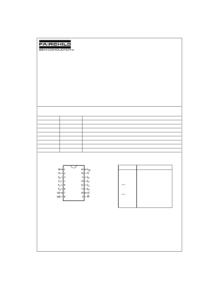
Connection Diagram
Pin Descriptions
Order Number
Package Number
Package Description
74AC163SC
M16A
16-Lead Small Outline Integrated Circuit (SOIC), JEDEC MS-012, 0.150" Narrow Body
74AC163SJ
M16D
16-Lead Small Outline Package, (SOP), EIAJ TYPE II, 5.3mm Wide
74AC163MTC
MTC16
16-Lead Thin Shrink Small Outline Package (TSSOP), JEDEC MO-153, 4.4mm Wide
74AC163PC
N16E
16-Lead Plastic Dual-In-Line Package (PDIP), JEDEC MS-001, 0.300" Wide
74ACT163SC
M16A
16-Lead Small Outline Integrated Circuit (SOIC), JEDEC MS-012, 0.150" Narrow Body
74ACT163SJ
M16D
16-Lead Small Outline Package, (SOP), EIAJ TYPE II, 5.3mm Wide
74ACT163MTC
MTC16
16-Lead Thin Shrink Small Outline Package (TSSOP), JEDEC MO-153, 4.4mm Wide
74ACT163PC
N16E
16-Lead Plastic Dual-In-Line Package (PDIP), JEDEC MS-001, 0.300" Wide
Pin Names
Description
CEP
Count Enable Parallel Input
CET
Count Enable Trickle Input
CP
Clock Pulse Input
SR
Synchronous Reset Input
P
0
≠P
3
Parallel Data Inputs
PE
Parallel Enable Input
Q
0
≠Q
3
Flip-Flop Outputs
TC
Terminal Count Output
www.fairchildsemi.com
2
74AC163
∑ 74ACT163
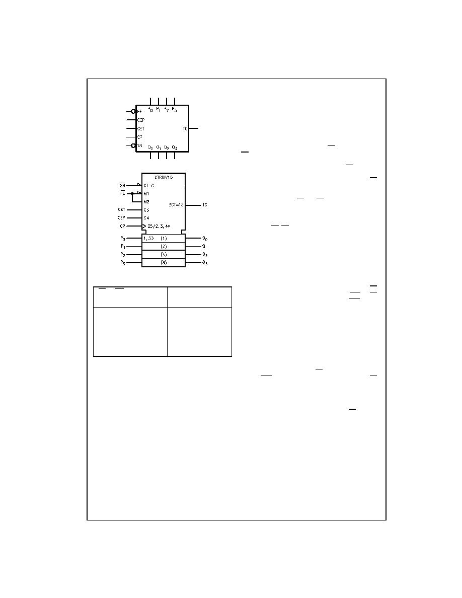
Logic Symbols
IEEE/IEC
Mode Select Table
H
=
HIGH Voltage Level
L
=
LOW Voltage Level
X
=
Immaterial
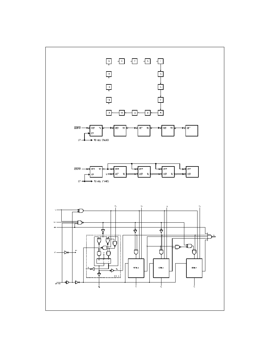
Functional Description
The AC/ACT163 counts in modulo-16 binary sequence.
From state 15 (HHHH) it increments to state 0 (LLLL). The
clock inputs of all flip-flops are driven in parallel through a
clock buffer. Thus all changes of the Q outputs occur as a
result of, and synchronous with, the LOW-to-HIGH transi-
tion of the CP input signal. The circuits have four funda-
mental modes of operation, in order of precedence:
synchronous reset, parallel load, count-up and hold. Four
control inputs--Synchronous Reset (SR), Parallel Enable
(PE), Count Enable Parallel (CEP) and Count Enable
Trickle (CET)--determine the mode of operation, as shown
in the Mode Select Table. A LOW signal on SR overrides
counting and parallel loading and allows all outputs to go
LOW on the next rising edge of CP. A LOW signal on PE
overrides counting and allows information on the Parallel
Data (P
n
) inputs to be loaded into the flip-flops on the next
rising edge of CP. With PE and SR HIGH, CEP and CET
permit counting when both are HIGH. Conversely, a LOW
signal on either CEP or CET inhibits counting.
The AC/ACT163 uses D-type edge-triggered flip-flops and
changing the SR, PE, CEP and CET inputs when the CP is
in either state does not cause errors, provided that the rec-
ommended setup and hold times, with respect to the rising
edge of CP, are observed.
The Terminal Count (TC) output is HIGH when CET is
HIGH and counter is in state 15. To implement synchro-
nous multistage counters, the TC outputs can be used with
the CEP and CET inputs in two different ways.
Figure 1 shows the connections for simple ripple carry, in
which the clock period must be longer than the CP to TC
delay of the first stage, plus the cumulative CET to TC
delays of the intermediate stages, plus the CET to CP
setup time of the last stage. This total delay plus setup time
sets the upper limit on clock frequency. For faster clock
rates, the carry lookahead connections shown in Figure 2
are recommended. In this scheme the ripple delay through
the intermediate stages commences with the same clock
that causes the first stage to tick over from max to min in
the Up mode, or min to max in the Down mode, to start its
final cycle. Since this final cycle takes 16 clocks to com-
plete, there is plenty of time for the ripple to progress
through the intermediate stages. The critical timing that lim-
its the clock period is the CP to TC delay of the first stage
plus the CEP to CP setup time of the last stage. The TC
output is subject to decoding spikes due to internal race
conditions and is therefore not recommended for use as a
clock or asynchronous reset for flip-flops, registers or
counters.
Logic Equations: Count Enable
=
CEP ∑ CET ∑ PE
TC
=
Q
0
∑ Q
1
∑ Q
2
∑ Q
3
∑ CET
SR
PE
CET
CEP
Action on the Rising
Clock Edge (
)
L
X
X
X
Reset (Clear)
H
L
X
X
Load (P
n
Q
n
)
H
H
H
H
Count (Increment)
H
H
L
X
No Change (Hold)
H
H
X
L
No Change (Hold)
3
www.fairchildsemi.com
74
A
C
16
3
∑ 74ACT163
State Diagram
FIGURE 1.
FIGURE 2.
Block Diagram
Please note that this diagram is provided only for the understanding of logic operations and should not be used to estimate propagation delays.
www.fairchildsemi.com
4
74AC163
∑ 74ACT163
Absolute Maximum Ratings
(Note 1)
Recommended Operating
Conditions
Note 1: Absolute maximum ratings are those values beyond which damage
to the device may occur. The databook specifications should be met, with-
out exception, to ensure that the system design is reliable over its power
supply, temperature, and output/input loading variables. Fairchild does not
recommend operation of circuits outside databook specifications.
DC Electrical Characteristics for AC
Note 2: All outputs loaded; thresholds on input associated with output under test.
Note 3: Maximum test duration 2.0 ms, one output loaded at a time.
Note 4: I
IN
and I
CC
@ 3.0V are guaranteed to be less than or equal to the respective limit @ 5.5V V
CC
.
Supply Voltage (V
CC
)
-
0.5V to
+
7.0V
DC Input Diode Current (I
IK
)
V
I
=
-
0.5V
-
20 mA
V
I
=
V
CC
+
0.5V
+
20 mA
DC Input Voltage (V
I
)
-
0.5V to V
CC
+
0.5V
DC Output Diode Current (I
OK
)
V
O
=
-
0.5V
-
20 mA
V
O
=
V
CC
+
0.5V
+
20 mA
DC Output Voltage (V
O
)
-
0.5V to V
CC
+
0.5V
DC Output Source
or Sink Current (I
O
)
±
50 mA
DC V
CC
or Ground Current
per Output Pin (I
CC
or I
GND
)
±
50 mA
Storage Temperature (T
STG
)
-
65
∞
C to
+
150
∞
C
Junction Temperature (T
J
)
PDIP
140
∞
C
Supply Voltage (V
CC
)
AC
2.0V to 6.0V
ACT
4.5V to 5.5V
Input Voltage (V
I
)
0V to V
CC
Output Voltage (V
O
)
0V to V
CC
Operating Temperature (T
A
)
-
40
∞
C to
+
85
∞
C
Minimum Input Edge Rate (
V/
t)
AC Devices
V
IN
from 30% to 70% of V
CC
V
CC
@ 3.3V, 4.5V, 5.5V
125 mV/ns
Minimum Input Edge Rate (
V/
t)
ACT Devices
V
IN
from 0.8V to 2.0V
V
CC
@ 4.5V, 5.5V
125 mV/ns
Symbol
Parameter
V
CC
T
A
=
+
25
∞
C T
A
=
-
40
∞
C to
+
85
∞
C
Units
Conditions
(V)
Typ
Guaranteed Limits
V
IH
Minimum HIGH Level
3.0
1.5
2.1
2.1
V
OUT
=
0.1V
Input Voltage
4.5
2.25
3.15
3.15
V
or V
CC
-
0.1V
5.5
2.75
3.85
3.85
V
IL
Maximum LOW Level
3.0
1.5
0.9
0.9
V
OUT
=
0.1V
Input Voltage
4.5
2.25
1.35
1.35
V
or V
CC
-
0.1V
5.5
2.75
1.65
1.65
V
OH
Minimum HIGH Level
3.0
2.99
2.9
2.9
Output Voltage
4.5
4.49
4.4
4.4
V
I
OUT
=
-
50
µ
A
5.5
5.49
5.4
5.4
V
IN
=
V
IL
or V
IH
3.0
2.56
2.46
I
OH
=
-
12 mA
4.5
3.86
3.76
V
I
OH
=
-
24 mA
5.5
4.86
4.76
I
OH
=
-
24 mA (Note 2)
V
OL
Maximum LOW Level
3.0
0.002
0.1
0.1
Output Voltage
4.5
0.001
0.1
0.1
V
I
OUT
=
50
µ
A
5.5
0.001
0.1
0.1
V
IN
=
V
IL
or V
IH
3.0
0.36
0.44
I
OL
= 12 mA
4.5
0.36
0.44
V
I
OL
= 24 mA
5.5
0.36
0.44
I
OL
= 24 mA (Note 2)
I
IN
(Note 4) Maximum Input Leakage Current
5.5
±
0.1
±
1.0
µ
A
V
I
=
V
CC
, GND
I
OLD
Minimum Dynamic
5.5
75
mA
V
OLD
=
1.65V Max
I
OHD
Output Current (Note 3)
5.5
-
75
mA
V
OHD
=
3.85V Min
I
CC
Maximum Quiescent
5.5
4.0
40.0
µ
A
V
IN
=
V
CC
(Note 4)
Supply Current
or GND
5
www.fairchildsemi.com
74
A
C
16
3
∑ 74ACT163
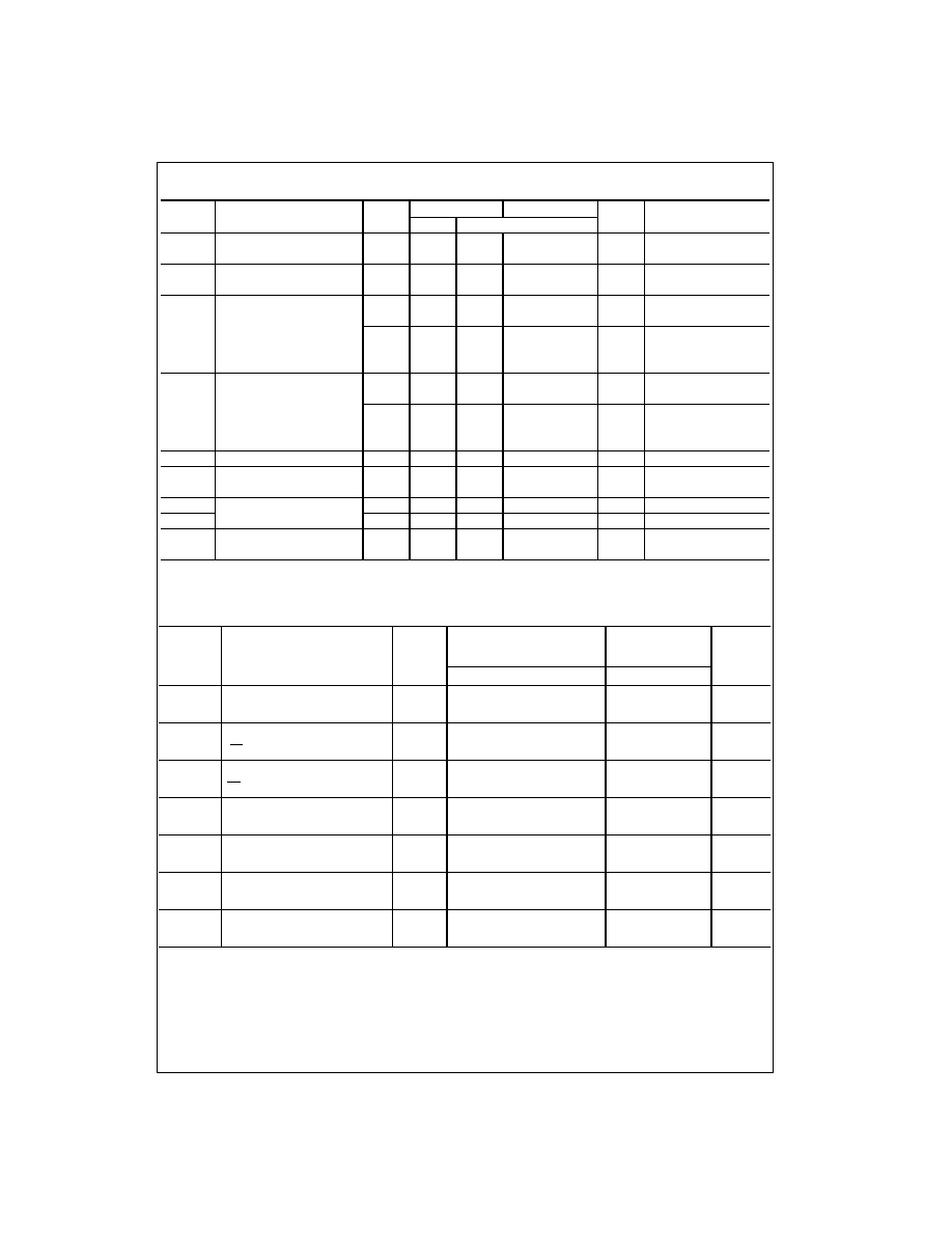
DC Electrical Characteristics for ACT
Note 5: All outputs loaded; thresholds on input associated with output under test.
Note 6: Maximum test duration 2.0 ms, one output loaded at a time.
AC Electrical Characteristics for AC
Note 7: Voltage Range 3.3 is 3.3V
±
0.3V
Voltage Range 5.0 is 5.0V
±
0.5V
Symbol
Parameter
V
CC
T
A
=
+
25
∞
C T
A
=
-
40
∞
C to
+
85
∞
C
Units
Conditions
(V)
Typ
Guaranteed Limits
V
IH
Minimum HIGH Level
4.5
1.5
2.0
2.0
V
V
OUT
=
0.1V
Input Voltage
5.5
1.5
2.0
2.0
or V
CC
-
0.1V
V
IL
Maximum LOW Level
4.5
1.5
0.8
0.8
V
V
OUT
=
0.1V
Input Voltage
5.5
1.5
0.8
0.8
or V
CC
-
0.1V
V
OH
Minimum HIGH Level
4.5
4.49
4.4
4.4
V
I
OUT
=
-
50
µ
A
Output Voltage
5.5
5.49
5.4
5.4
V
IN
=
V
IL
or V
IH
4.5
3.86
3.76
V
I
OH
=
-
24 mA
5.5
4.86
4.76
I
OH
=
-
24 mA (Note 5)
V
OL
Maximum LOW Level
4.5
0.001
0.1
0.1
V
I
OUT
=
50
µ
A
Output Voltage
5.5
0.001
0.1
0.1
V
IN
=
V
IL
or V
IH
4.5
0.36
0.44
V
I
OL
= 24 mA
5.5
0.36
0.44
I
OL
= 24 mA (Note 5)
I
IN
Maximum Input Leakage Current
5.5
±
0.1
±
1.0
µ
A
V
I
=
V
CC
, GND
I
CCT
Maximum
5.5
0.6
1.5
mA
V
I
=
V
CC
-
2.1V
I
CC
/Input
I
OLD
Minimum Dynamic
5.5
75
mA
V
OLD
=
1.65V Max
I
OHD
Output Current (Note 6)
5.5
-
75
mA
V
OHD
=
3.85V Min
I
CC
Maximum Quiescent
5.5
4.0
40.0
µ
A
V
IN
=
V
CC
Supply Current
or GND
V
CC
T
A
=
+
25
∞
C
T
A
=
-
40
∞
C to
+
85
∞
C
Symbol
Parameter
(V)
C
L
=
50 pF
C
L
=
50 pF
Units
(Note 7)
Min
Typ
Max
Min
Max
f
MAX
Maximum
Clock 3.3
70
95
60
MHz
Frequency
5.0
110
140
95
t
PLH
Propagation Delay, CP to Q
n
3.3
2.0
7.5
12.5
1.5
13.5
ns
(PE Input HIGH or LOW)
5.0
1.5
5.5
9.0
1.0
9.5
t
PHL
Propagation Delay, CP to Q
n
3.3
1.5
8.5
12.0
1.5
13.0
ns
(PE Input HIGH or LOW)
5.0
1.5
6.0
9.5
1.5
10.0
t
PLH
Propagation Delay
3.3
3.0
9.5
15.0
2.5
16.5
ns
CP to TC
5.0
2.0
7.0
10.5
1.5
11.5
t
PHL
Propagation Delay
3.3
3.5
11.0
14.0
2.5
15.5
ns
CP to TC
5.0
2.0
8.0
11.0
2.0
11.5
t
PLH
Propagation Delay
3.3
2.0
7.5
9.5
1.5
11.0
ns
CET to TC
5.0
1.5
5.5
6.5
1.0
7.5
t
PHL
Propagation Delay
3.3
2.5
8.5
11.0
2.0
12.5
ns
CET to TC
5.0
2.0
6.0
8.5
1.5
9.5