© 1999 Fairchild Semiconductor Corporation
DS500300
www.fairchildsemi.com
August 1999
Revised October 1999
7
4
AC
T1
6541
1
6
-Bi
t
Buff
er/
L
ine Dri
ver wit
h
3-
ST
A
T
E Output
s
74ACT16541
16-Bit Buffer/Line Driver with 3-STATE Outputs
General Description
The ACT16541 contains sixteen non-inverting buffers with
3-STATE outputs designed to be employed as a memory
and address driver, clock driver, or bus oriented transmit-
ter/receiver. The device is byte controlled. Each byte has
separate 3-STATE control inputs which can be shorted
together for full 16-bit operation.
Features
s
Separate control logic for each byte
s
Outputs source/sink 24 mA
s
TTL-compatible inputs
Ordering Code:
Device also available in Tape and Reel. Specify by appending suffix letter "X" to the ordering code.
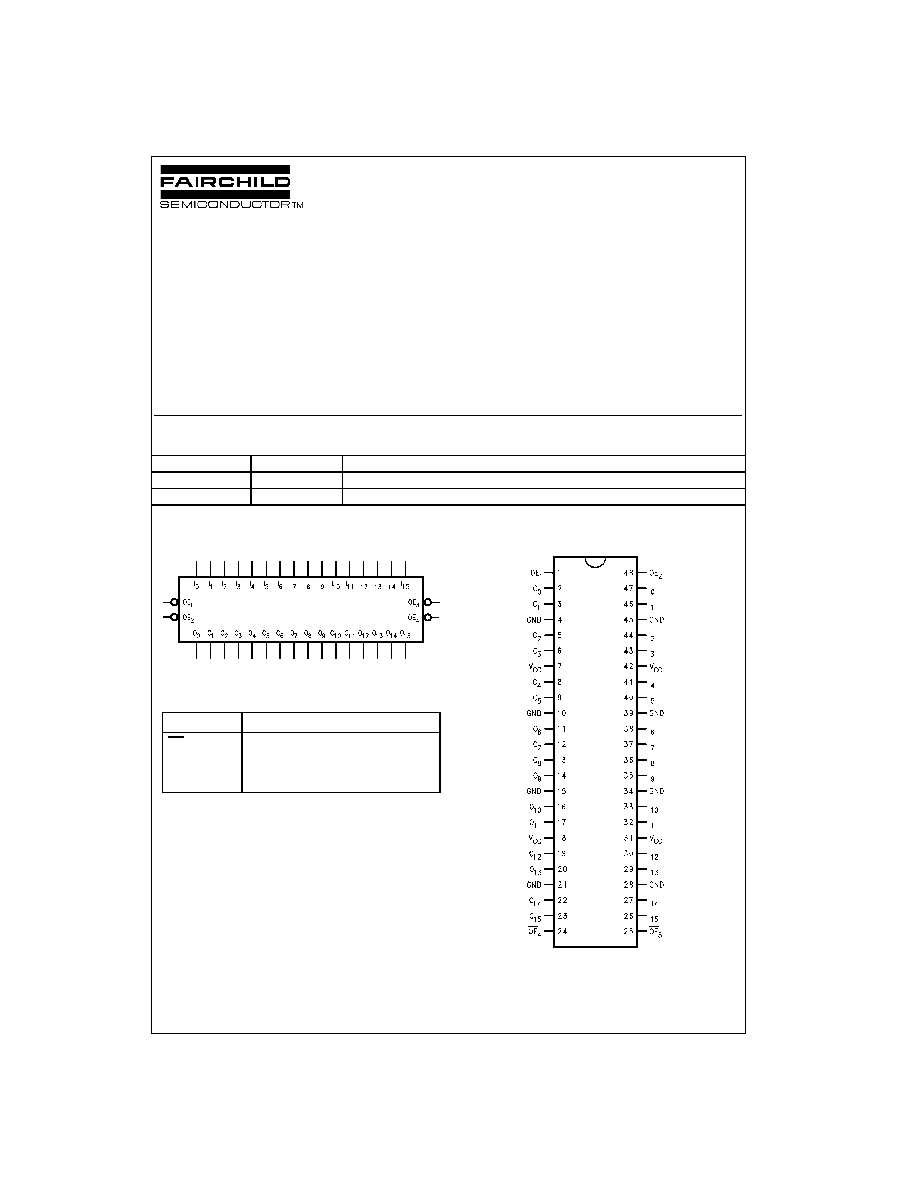
Logic Symbol
Pin Descriptions
Connection Diagram
FACT
TM
is a trademark of Fairchild Semiconductor Corporation
Order Number
Package Number
Package Description
74ACT16541SSC
MS48A
48-Lead Small Shrink Outline Package (SSOP), JEDEC MO-118, 0.300" Wide
74ACT16541MTD
MTD48
48-Lead Thin Shrink Small Outline Package (TSSOP), MO-153, 6.1mm Wide
Pin Names
Description
OE
n
Output Enable Input (Active LOW)
I
0
≠I
15
Inputs
O
0
≠O
15
Outputs

www.fairchildsemi.com
2
74ACT16541
Functional Description
The ACT16541 contains sixteen non-inverting buffers with
3-STATE standard outputs. The device is byte controlled
with each byte functioning identically, but independent of
the other. The control pins can be shorted together to
obtain full 16-bit operation. The 3-STATE outputs are con-
trolled by an Output Enable (OE
n
) input for each byte.
When OE
n
is LOW, the outputs are in 2-state mode. When
OE
n
is HIGH, the outputs are in the high impedance mode,
but this does not interfere with entering new data into the
inputs.
Truth Tables
H = HIGH Voltage Level
L = LOW Voltage Level
X = Immaterial
Z = High Impedance
Logic Diagram
Inputs
Outputs
OE
1
OE
2
I
0
≠I
7
O
0
≠O
7
L
L
H
H
H
X
X
Z
X
H
X
Z
L
L
L
L
Inputs
Outputs
OE
3
OE
4
I
8
≠I
15
O
8
≠O
15
L
L
H
H
H
X
X
Z
X
H
X
Z
L
L
L
L

3
www.fairchildsemi.com
7
4
AC
T1
6541
Absolute Maximum Ratings
(Note 1)
Recommended Operating
Conditions
Note 1: Absolute maximum ratings are those values beyond which damage
to the device may occur. The databook specifications should be met, with-
out exception to ensure that the system design is reliable over its power
supply, temperature, and output/input loading variables. Fairchild does not
recommend operation of FACT
TM
circuits outside databook specifications.
DC Electrical Characteristics
Note 2: All outputs loaded; thresholds associated with output under test.
Note 3: Maximum test duration 2.0 ms; one output loaded at a time.
Supply Voltage (V
CC
)
-
0.5V to +7.0V
DC Input Diode Current (I
IK
)
V
I
=
-
0.5V
-
20 mA
V
I
= V
CC
+ 0.5V
+20 mA
DC Output Diode Current (I
OK
)
V
O
=
-
0.5V
-
20 mA
V
O
= V
CC
+ 0.5V
+20 mA
DC Output Voltage (V
O
)
-
0.5V to V
CC
+ 0.5V
DC Output Source/Sink Current (I
O
)
±
50 mA
DC V
CC
or Ground Current
per Output Pin
±
50 mA
Storage Temperature
-
65
∞
C to +150
∞
C
Supply Voltage (V
CC
)
4.5V to 5.5V
Input Voltage (V
I
)
0V to V
CC
Output Voltage (V
O
)
0V to V
CC
Operating Temperature (T
A
)
-
40
∞
C to +85
∞
C
Minimum Input Edge Rate (
V/
t)
125 mV/ns
V
IN
from 0.8V to 2.0V
V
CC
@ 4.5V, 5.5V
Symbol
Parameter
V
CC
T
A
= +25
∞
C
T
A
=
-
40
∞
C to +85
∞
C
Units
Conditions
(V)
Typ
Guaranteed Limits
V
IH
Minimum HIGH
4.5
1.5
2.0
2.0
V
V
OUT
= 0.1V
Input Voltage
5.5
1.5
2.0
2.0
or V
CC
-
0.1V
V
IL
Maximum LOW
4.5
1.5
0.8
0.8
V
V
OUT
= 0.1V
Input Voltage
5.5
1.5
0.8
0.8
or V
CC
-
0.1V
V
OH
Minimum HIGH
4.5
4.49
4.4
4.4
V
I
OUT
=
-
50
µ
A
Output Voltage
5.5
5.49
5.4
5.4
V
IN
= V
IL
or V
IH
4.5
3.86
3.76
V
I
OH
=
-
24 mA
5.5
4.86
4.76
I
OH
=
-
24 mA (Note 2)
V
OL
Maximum LOW
4.5
0.001
0.1
0.1
V
I
OUT
= 50
µ
A
Output Voltage
5.5
0.001
0.1
0.1
V
IN
= V
IL
or V
IH
4.5
0.36
0.44
V
I
OL
= 24 mA
5.5
0.36
0.44
I
OL
= 24 mA (Note 2)
I
OZ
Maximum 3-STATE
5.5
±
0.5
±
5.0
µ
A
V
I
= V
IL
, V
IH
Leakage Current
V
O
= V
CC
, GND
I
IN
Maximum Input
5.5
±
0.1
±
1.0
µ
A
V
I
= V
CC
, GND
Leakage Current
I
CCT
Maximum I
CC
/Input
5.5
0.6
1.5
mA
V
I
= V
CC
-
2.1V
I
CC
Max Quiescent
5.5
8.0
80.0
µ
A
V
IN
= V
CC
or GND
Supply Current
I
OLD
Minimum Dynamic
5.5
75
mA
V
OLD
= 1.65V Max
I
OHD
Output Current (Note 3)
-
75
mA
V
OHD
= 3.85V Min
www.fairchildsemi.com
4
74ACT16541
AC Electrical Characteristics
Note 4: Voltage Range 5.0 is 5.0V
±
0.5V.
Capacitance
V
CC
T
A
= +25
∞
C
T
A
=
-
40
∞
C to +85
∞
C
Symbol
Parameter
(V)
C
L
= 50 pF
C
L
= 50 pF
Units
(Note 4)
Min
Typ
Max
Min
Max
t
PLH
Propagation Delay
5.0
3.0
5.2
7.3
3.0
7.8
ns
t
PHL
Data to Output
2.5
4.8
7.3
2.5
7.8
t
PZH
Output Enable Time
5.0
2.6
5.0
7.4
2.6
7.9
ns
t
PZL
2.7
5.4
8.0
2.7
8.5
t
PHZ
Output Disable Time
5.0
2.7
5.6
8.3
2.7
8.7
ns
t
PLZ
2.4
5.2
7.9
2.4
8.4
Symbol
Parameter
Typ
Units
Conditions
C
IN
Input Capacitance
4.5
pF
V
CC
= 5.0V
C
PD
Power Dissipation Capacitance
30
pF
V
CC
= 5.0V
5
www.fairchildsemi.com
7
4
AC
T1
6541
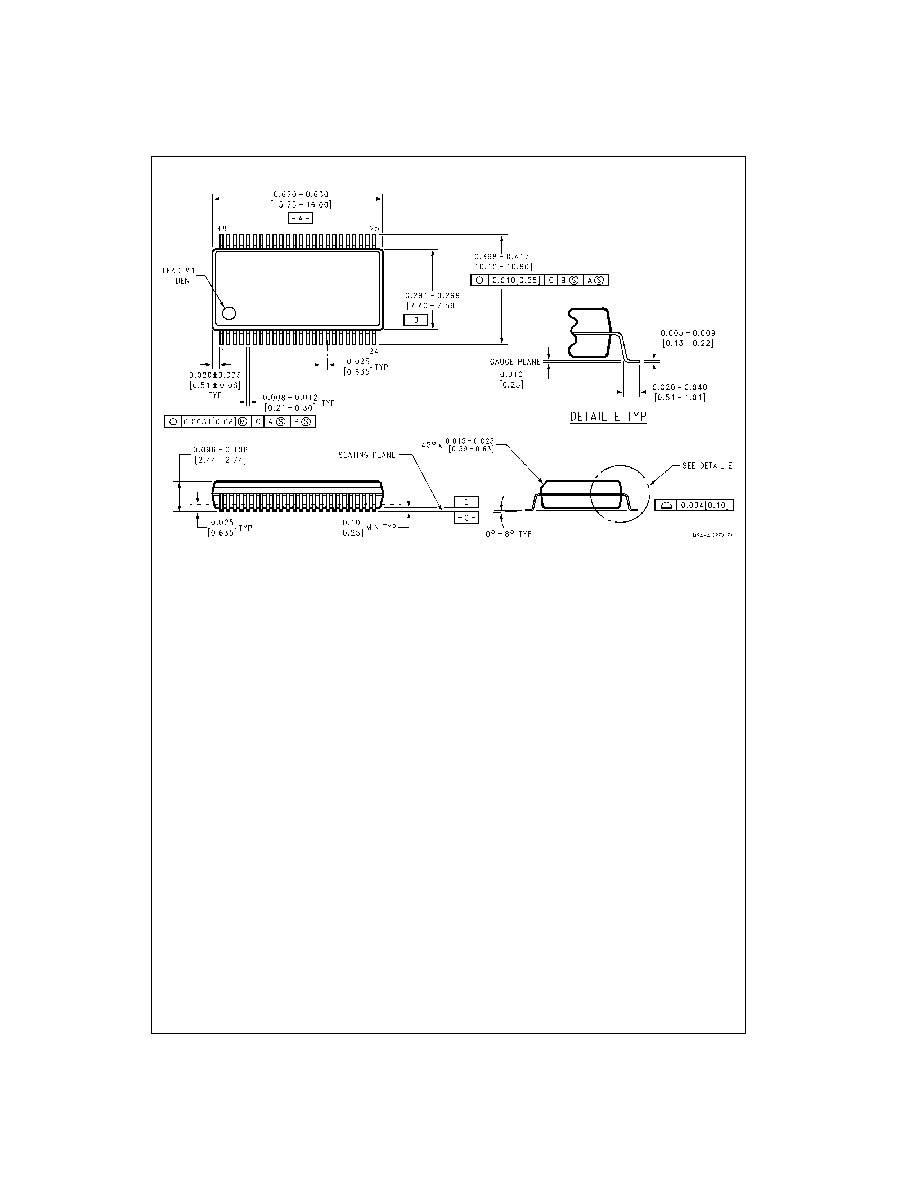
Physical Dimensions
inches (millimeters) unless otherwise noted
48-Lead Small Shrink Outline Package (SSOP), JEDEC MO-118, 0.300" Wide
Package Number MS48A