© 2005 Fairchild Semiconductor Corporation
DS009942
www.fairchildsemi.com
November 1988
Revised March 2005
7
4
AC
2
41
∑ 74ACT241 O
c
t
a
l Buff
er/
L
ine
Dri
ver wit
h
3
-
ST
A
T
E
Output
s
74AC241 ∑ 74ACT241
Octal Buffer/Line Driver with 3-STATE Outputs
General Description
The AC/ACT241 is an octal buffer and line driver designed
to be employed as a memory address driver, clock driver
and bus-oriented transmitter or receiver which provides
improved PC board density.
Features
s
I
CC
and I
OZ
reduced by 50%
s
Non-inverting 3-STATE outputs drive bus lines or buffer
memory address registers
s
Outputs source/sink 24 mA
s
ACT241 has TTL-compatible inputs
Ordering Code:
Device also available in Tape and Reel. Specify by appending suffix letter "X" to the ordering code.
Pb-Free package per JEDEC J-STD-020B.
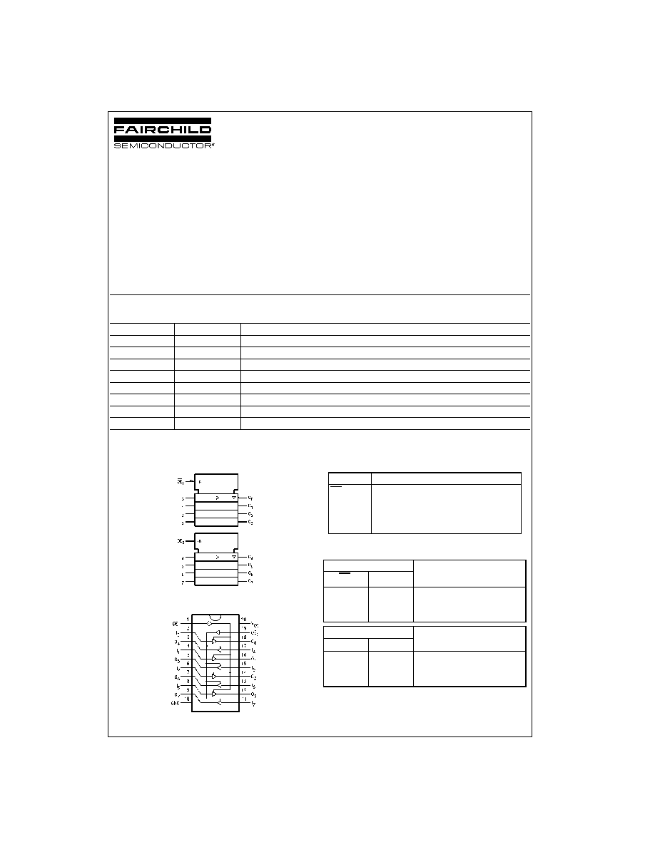
Logic Symbol
Connection Diagram
Pin Descriptions
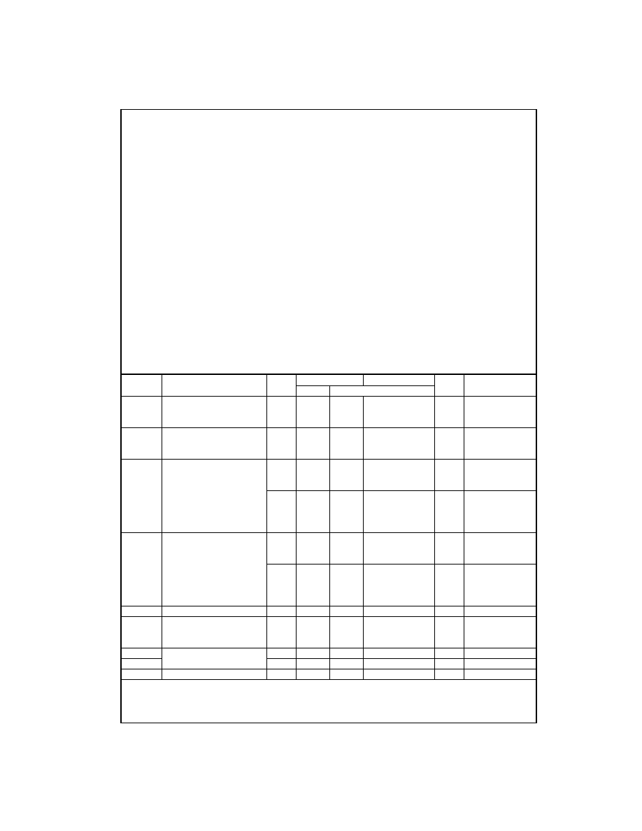
Truth Tables
H
HIGH Voltage Level
L
LOW Voltage Level
X
Immaterial
Z
High Impedance
FACT
•
is a trademark of Fairchild Semiconductor Corporation.
Order Number
Package Number
Package Description
74AC241SC
M20B
20-Lead Small Outline Integrated Circuit (SOIC), JEDEC MS-013, 0.300" Wide
74AC241SJ
M20D
Pb-Free 20-Lead Small Outline Package (SOP), EIAJ TYPE II, 5.3mm Wide
74AC241MTC
MTC20
20-Lead Thin Shrink Small Outline Package (TSSOP), JEDEC MO-153, 4.4mm Wide
74AC241PC
N20A
20-Lead Plastic Dual-In-Line Package (PDIP), JEDEC MS-001, 0.300" Wide
74ACT241SC
M20B
20-Lead Small Outline Integrated Circuit (SOIC), JEDEC MS-013, 0.300" Wide
74ACT241SJ
M20D
Pb-Free 20-Lead Small Outline Package (SOP), EIAJ TYPE II, 5.3mm Wide
74ACT241MTC
MTC20
20-Lead Thin Shrink Small Outline Package (TSSOP), JEDEC MO-153, 4.4mm Wide
74ACT241PC
N20A
20-Lead Plastic Dual-In-Line Package (PDIP), JEDEC MS-001, 0.300" Wide
Pin Names
Description
OE
1
3-STATE Output Enable Input
OE
2
3-STATE Output Enable Input (Active HIGH)
I
0
≠I
7
Inputs
O
0
≠O
7
Outputs
Inputs
Outputs
OE
1
I
n
(Pins 12, 14, 16, 18)
L
L
L
L
H
H
H
X
Z
Inputs
Outputs
OE
2
I
n
(Pins 3, 5, 7, 9)
H
L
L
H
H
H
L
X
Z
www.fairchildsemi.com
2
74AC241
∑
74ACT241
Absolute Maximum Ratings
(Note 1)
Recommended Operating
Conditions
Note 1: Absolute maximum ratings are those values beyond which damage
to the device may occur. The databook specifications should be met, with-
out exception, to ensure that the system design is reliable over its power
supply, temperature, and output/input loading variables. Fairchild does not
recommend operation of FACT
•
circuits outside databook specifications.
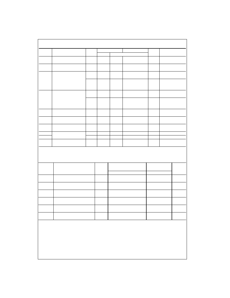
DC Electrical Characteristics for AC
Note 2: All outputs loaded; thresholds on input associated with output under test.
Note 3: Maximum test duration 2.0 ms, one output loaded at a time.
Note 4: I
IN
and I
CC
@ 3.0V are guaranteed to be less than or equal to the respective limit @ 5.5V V
CC
.
Supply Voltage (V
CC
)
0.5V to
7.0V
DC Input Diode Current (I
IK
)
V
I
0.5V
20 mA
V
I
V
CC
0.5V
20 mA
DC Input Voltage (V
I
)
0.5V to V
CC
0.5V
DC Output Diode Current (I
OK
)
V
O
0.5V
20 mA
V
O
V
CC
0.5V
20 mA
DC Output Voltage (V
O
)
0.5V to V
CC
0.5V
DC Output Source
or Sink Current (I
O
)
r
50 mA
DC V
CC
or Ground Current
per Output Pin (I
CC
or I
GND
)
r
50 mA
Storage Temperature (T
STG
)
65
q
C to
150
q
C
Junction Temperature (T
J
)
PDIP
140
q
C
Supply Voltage (V
CC
)
AC
2.0V to 6.0V
ACT
4.5V to 5.5V
Input Voltage (V
I
)
0V to V
CC
Output Voltage (V
O
)
0V to V
CC
Operating Temperature (T
A
)
40
q
C to
85
q
C
Minimum Input Edge Rate (
'
V/
'
t)
AC Devices
V
IN
from 30% to 70% of V
CC
V
CC
@ 3.3V, 4.5V, 5.5V
125 mV/ns
Minimum Input Edge Rate (
'
V/
'
t)
ACT Devices
V
IN
from 0.8V to 2.0V
V
CC
@ 4.5V, 5.5V
125 mV/ns
Symbol
Parameter
V
CC
T
A
25
q
C
T
A
40
q
C to
85
q
C
Units
Conditions
(V)
Typ
Guaranteed Limits
V
IH
Minimum HIGH Level
3.0
1.5
2.1
2.1
V
OUT
0.1V
Input Voltage
4.5
2.25
3.15
3.15
V
or V
CC
0.1V
5.5
2.75
3.85
3.85
V
IL
Maximum LOW Level
3.0
1.5
0.9
0.9
V
OUT
0.1V
Input Voltage
4.5
2.25
1.35
1.35
V
or V
CC
0.1V
5.5
2.75
1.65
1.65
V
OH
Minimum HIGH Level
3.0
2.99
2.9
2.9
Output Voltage
4.5
4.49
4.4
4.4
V
I
OUT
50
P
A
5.5
5.49
5.4
5.4
V
IN
V
IL
or V
IH
3.0
2.56
2.46
I
OH
12 mA
4.5
3.86
3.76
V
I
OH
24 mA
5.5
4.86
4.76
I
OH
24 mA (Note 2)
V
OL
Maximum LOW Level
3.0
0.002
0.1
0.1
Output Voltage
4.5
0.001
0.1
0.1
V
I
OUT
50
P
A
5.5
0.001
0.1
0.1
V
IN
V
IL
or V
IH
3.0
0.36
0.44
I
OL
12 mA
4.5
0.36
0.44
V
I
OL
24 mA
5.5
0.36
0.44
I
OL
24 mA (Note 2)
I
N
(Note 4)
Maximum Input Leakage Current
5.5
r
0.1
r
1.0
P
A
V
I
V
CC
, GND
I
OZ
Maximum 3-STATE
V
I
(OE)
V
IL
, V
IH
Leakage Current
5.5
r
0.25
r
2.5
P
A
V
I
V
CC
, GND
V
O
V
CC
, GND
I
OLD
Minimum Dynamic
5.5
75
mA
V
OLD
1.65V Max
I
OHD
Output Current (Note 3)
5.5
75
mA
V
OHD
3.85V Min
I
CC
(Note 4)
Maximum Quiescent Supply Current
5.5
4.0
40.0
P
A
V
IN
V
CC
or GND
3
www.fairchildsemi.com
74
A
C
24
1
∑
74ACT241
DC Electrical Characteristics for ACT
Note 5: All outputs loaded; thresholds on input associated with output under test.
Note 6: Maximum test duration 2.0 ms, one output loaded at a time.
AC Electrical Characteristics for AC
Note 7: Voltage Range 3.3 is 3.3V
r
3.3V
Voltage Range 5.0 is 5.0V
r
0.5V
Symbol
Parameter
V
CC
T
A
25
q
C
T
A
40
q
C to
85
q
C
Units
Conditions
(V)
Typ
Guaranteed Limits
V
IH
Minimum HIGH Level
4.5
1.5
2.0
2.0
V
V
OUT
0.1V
Input Voltage
5.5
1.5
2.0
2.0
or V
CC
0.1V
V
IL
Maximum LOW Level
4.5
1.5
0.8
0.8
V
V
OUT
0.1V
Input Voltage
5.5
1.5
0.8
0.8
or V
CC
0.1V
V
OH
Minimum HIGH Level
4.5
4.49
4.4
4.4
V
I
OUT
50
P
A
Output Voltage
5.5
5.49
5.4
5.4
V
IN
V
IL
or V
IH
4.5
3.86
3.76
V
I
OH
24 mA
5.5
4.86
4.76
I
OH
24 mA (Note 5)
V
OL
Maximum LOW Level
4.5
0.001
0.1
0.1
V
I
OUT
50
P
A
Output Voltage
5.5
0.001
0.1
0.1
V
IN
V
IL
or V
IH
4.5
0.36
0.44
V
I
OL
24 mA
5.5
0.36
0.44
I
OL
24 mA (Note 5)
I
IN
Maximum Input
5.5
r
0.1
r
1.0
P
A
V
I
V
CC
, GND
Leakage Current
I
OZ
Maximum 3-STATE
5.5
r
0.25
r
2.5
P
A
V
I
V
IL
, V
IH
Leakage Current
V
O
V
CC
, GND
I
CCT
Maximum
5.5
0.6
1.5
mA
V
I
V
CC
2.1V
I
CC
/Input
I
OLD
Minimum Dynamic
5.5
75
mA
V
OLD
1.65V Max
I
OHD
Output Current (Note 6)
5.5
75
mA
V
OHD
3.85V Min
I
CC
Maximum Quiescent
5.5
4.0
40.0
P
A
V
IN
V
CC
Supply Current
or GND
V
CC
T
A
25
q
C
T
A
40
q
C to
85
q
C
Symbol
Parameter
(V)
C
L
50 pF
C
L
50 pF
Units
(Note 7)
Min
Typ
Max
Min
Max
t
PLH
Propagation Delay
3.3
1.5
6.0
9.0
1.5
10.0
ns
Data to Output
5.0
1.5
5.0
7.0
1.0
7.5
t
PHL
Propagation Delay
3.3
1.5
6.0
9.0
1.0
10.5
ns
Data to Output
5.0
1.5
4.5
7.0
1.0
7.5
t
PZH
Output Enable Time
3.3
1.5
6.5
12.5
1.0
13.0
ns
5.0
1.5
5.5
9.0
1.0
9.5
t
PZL
Output Enable Time
3.3
1.5
7.0
12.0
1.5
13.0
ns
5.0
1.5
5.5
9.0
1.0
9.5
t
PHZ
Output Disable Time
3.3
2.0
8.0
12.0
2.0
12.5
ns
5.0
1.5
6.5
10.0
1.0
10.5
t
PLZ
Output Disable Time
3.3
1.5
7.0
12.5
1.0
13.0
ns
5.0
1.5
6.0
10.0
1.0
10.5
www.fairchildsemi.com
4
74AC241
∑
74ACT241
AC Electrical Characteristics for ACT
Note 8: Voltage Range 5.0 is 5.0V
r
0.5V
Capacitance
V
CC
T
A
25
q
C
T
A
40
q
C to
85
q
C
Symbol
Parameter
(V)
C
L
50 pF
C
L
50 pF
Units
(Note 8)
Min
Typ
Max
Min
Max
t
PLH
Propagation Delay
5.0
1.5
6.5
9.0
1.5
10.0
ns
Data to Output
t
PHL
Propagation Delay
5.0
1.5
7.0
9.0
1.5
10.0
ns
Data to Output
t
PZH
Output Enable Time
5.0
1.5
6.0
9.0
1.0
10.0
ns
t
PZL
Output Enable Time
5.0
1.5
7.0
10.0
1.5
11.0
ns
t
PHZ
Output Disable Time
5.0
1.5
8.0
10.5
1.5
11.5
ns
t
PLZ
Output Disable Time
5.0
2.0
7.0
10.5
1.5
11.5
ns
Symbol
Parameter
Typ
Units
Conditions
C
IN
Input Capacitance
4.5
pF
V
CC
OPEN
C
PD
Power Dissipation Capacitance
45.0
pF
V
CC
5.0V
5
www.fairchildsemi.com
74
A
C
24
1
∑
74ACT241
Physical Dimensions
inches (millimeters) unless otherwise noted
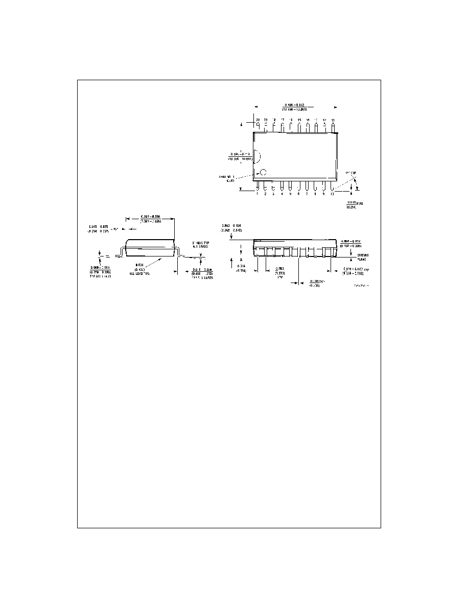
20-Lead Small Outline Integrated Circuit (SOIC), JEDEC MS-013, 0.300" Wide
Package Number M20B
www.fairchildsemi.com
6
74AC241
∑
74ACT241
Physical Dimensions
inches (millimeters) unless otherwise noted (Continued)
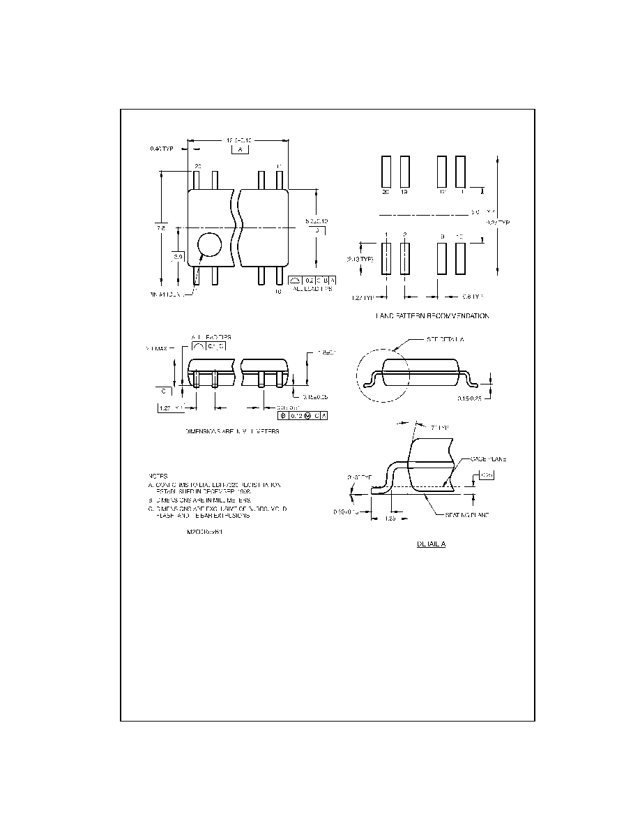
Pb-Free 20-Lead Small Outline Package (SOP), EIAJ TYPE II, 5.3mm Wide
Package Number M20D

7
www.fairchildsemi.com
74
A
C
24
1
∑
74ACT241
Physical Dimensions
inches (millimeters) unless otherwise noted (Continued)
20-Lead Thin Shrink Small Outline Package (TSSOP), JEDEC MO-153, 4.4mm Wide
Package Number MTC20
www.fairchildsemi.com
8
74
A
C
24
1
∑
74ACT241 O
c
t
a
l Buff
er/
L
ine Dri
ver wit
h
3-
ST
A
T
E Output
s
Physical Dimensions
inches (millimeters) unless otherwise noted (Continued)
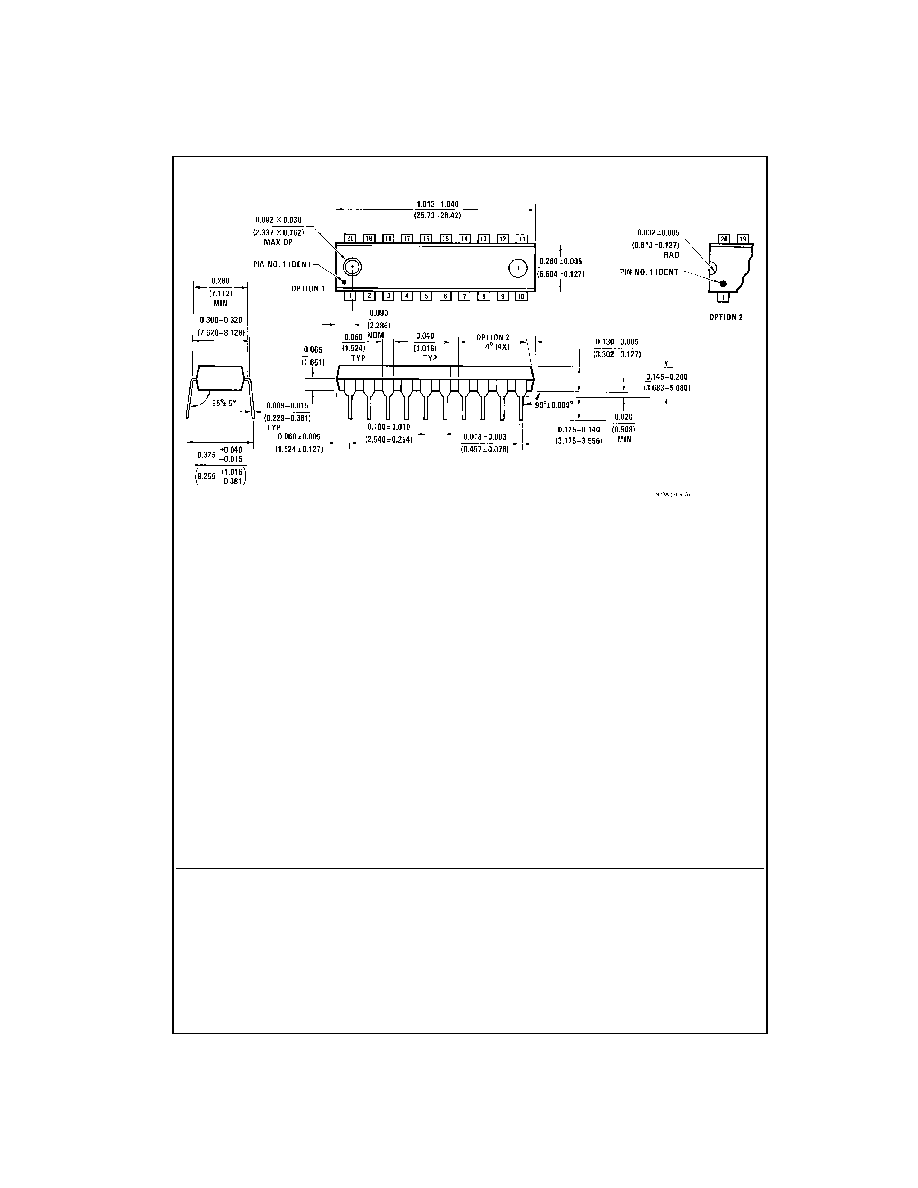
20-Lead Plastic Dual-In-Line Package (PDIP), JEDEC MS-001, 0.300" Wide
Package Number N20A
Fairchild does not assume any responsibility for use of any circuitry described, no circuit patent licenses are implied and
Fairchild reserves the right at any time without notice to change said circuitry and specifications.
LIFE SUPPORT POLICY
FAIRCHILD'S PRODUCTS ARE NOT AUTHORIZED FOR USE AS CRITICAL COMPONENTS IN LIFE SUPPORT
DEVICES OR SYSTEMS WITHOUT THE EXPRESS WRITTEN APPROVAL OF THE PRESIDENT OF FAIRCHILD
SEMICONDUCTOR CORPORATION. As used herein:
1. Life support devices or systems are devices or systems
which, (a) are intended for surgical implant into the
body, or (b) support or sustain life, and (c) whose failure
to perform when properly used in accordance with
instructions for use provided in the labeling, can be rea-
sonably expected to result in a significant injury to the
user.
2. A critical component in any component of a life support
device or system whose failure to perform can be rea-
sonably expected to cause the failure of the life support
device or system, or to affect its safety or effectiveness.
www.fairchildsemi.com