© 1999 Fairchild Semiconductor Corporation
DS009950
www.fairchildsemi.com
November 1988
Revised November 1999
7
4
AC
T2
58 Quad
2-I
nput
Mul
t
i
p
lexe
r wi
th
3-ST
A
T
E Out
puts
74ACT258
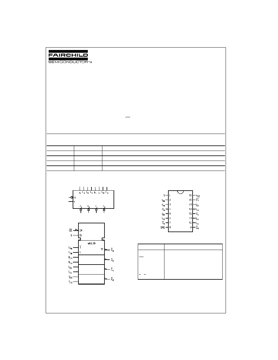
Quad 2-Input Multiplexer with 3-STATE Outputs
General Description
The ACT258 is a quad 2-input multiplexer with 3-STATE
outputs. Four bits of data from two sources can be selected
using a common data select input. The four outputs
present the selected data in the complement (inverted)
form. The outputs may be switched to a high impedance
state with a HIGH on the common Output Enable (OE)
input, allowing the outputs to interface directly with bus-ori-
ented systems.
Features
s
I
CC
and I
OZ
reduced by 50%
s
Multiplexer expansion by tying outputs together
s
Inverting 3-STATE outputs
s
Outputs source/sink 24 mA
s
TTL-compatible inputs
Ordering Code:
Device also available in Tape and Reel. Specify by appending suffix letter "X" to the ordering code.
Logic Symbols
IEEE/IEC
Connection Diagram
Pin Descriptions
FACT
is a trademark of Fairchild Semiconductor Corporation.
Order Number
Package Number
Package Description
74ACT258SC
M16A
16-Lead Small Outline Integrated Circuit (SOIC), JEDEC MS-012, 0.150" Narrow Body
74ACT258SJ
M16D
16-Lead Small Outline Package (SOP), EIAJ TYPE 11, 5.3mm Wide
74ACT258MTC
MTC16
16-Lead Thin Shrink Small Outline Package (TSSOP), JEDEC MO-153, 4.4mm Wide
74ACT258PC
N16E
16-Lead Plastic Dual-In-Line Package (PDIP), JEDEC MS-001, 0.300" Wide
Pin Names
Description
S
Common Data Select Input
OE
3-STATE Output Enable Input
I
0a
≠I
0d
Data Inputs from Source 0
I
1a
≠I
1d
Data Inputs from Source 1
Z
a
≠Z
d
3-STATE Inverting Data Outputs

www.fairchildsemi.com
2
74ACT258
Truth Table
H
=
HIGH Voltage Level
L
=
LOW Voltage Level
X
=
Immaterial
Z
=
High Impedance
Functional Description
The ACT258 is a quad 2-input multiplexer with 3-STATE
outputs. It selects four bits of data from two sources under
control of a common Select input (S). When the Select
input is LOW, the I
0x
inputs are selected and when Select
is HIGH, the I
1x
inputs are selected. The data on the
selected inputs appears at the outputs in inverted form.
The ACT258 is the logic implementation of a 4-pole, 2-
position switch where the position of the switch is deter-
mined by the logic levels supplied to the Select input. The
logic equations for the outputs are shown below:
Z
a
=
OE ∑ (I
1a
∑ S
+
I
0a
∑ S)
Z
b
=
OE ∑ (I
1b
∑ S
+
I
0b
∑ S)
Z
c
=
OE ∑ (I
1c
∑ S
+
I
0c
∑ S)
Z
d
=
OE ∑ (I
1d
∑ S
+
I
0d
∑ S)
When the Output Enable input (OE) is HIGH, the outputs
are forced to a high impedance state. If the outputs of the
3-STATE devices are tied together, all but one device must
be in the high impedance state to avoid high currents that
would exceed the maximum ratings. Designers should
ensure that Output Enable signals to 3-STATE devices
whose outputs are tied together are designed so there is
no overlap.
Logic Diagram
Please note that this diagram is provided only for the understanding of logic operations and should not be used to estimate propagation delays.
Output
Select
Data
Outputs
Enable
Input
Inputs
OE
S
I
0
I
1
Z
H
X
X
X
Z
L
H
X
L
H
L
H
X
H
L

3
www.fairchildsemi.com
74
A
C
T
2
5
8
Absolute Maximum Ratings
(Note 1)
Recommended Operating
Conditions
Note 1: Absolute maximum ratings are those values beyond which damage
to the device may occur. The databook specifications should be met, with-
out exception, to ensure that the system design is reliable over its power
supply, temperature, and output/input loading variables. Fairchild does not
recommend operation of FACT
circuits outside databook specifications.
DC Electrical Characteristics
Note 2: All outputs loaded; thresholds on input associated with output under test.
Note 3: Maximum test duration 2.0 ms, one output loaded at a time.
Supply Voltage (V
CC
)
-
0.5V to
+
7.0V
DC Input Diode Current (I
IK
)
V
I
=
-
0.5V
-
20 mA
V
I
=
V
CC
+
0.5V
+
20 mA
DC Input Voltage (V
I
)
-
0.5V to V
CC
+
0.5V
DC Output Diode Current (I
OK
)
V
O
=
-
0.5V
-
20 mA
V
O
=
V
CC
+
0.5V
+
20 mA
DC Output Voltage (V
O
)
-
0.5V to V
CC
+
0.5V
DC Output Source
or Sink Current (I
O
)
±
50 mA
DC V
CC
or Ground Current
per Output Pin (I
CC
or I
GND
)
±
50 mA
Storage Temperature (T
STG
)
-
65
∞
C to
+
150
∞
C
Junction Temperature (T
J
)
PDIP
140
∞
C
Supply Voltage (V
CC
)
4.5V to 5.5V
Input Voltage (V
I
)
0V to V
CC
Output Voltage (V
O
)
0V to V
CC
Operating Temperature (T
A
)
-
40
∞
C to
+
85
∞
C
Minimum Input Edge Rate (
V/
t)
V
IN
from 0.8V to 2.0V
V
CC
@ 4.5V, 5.5V
125 mV/ns
Symbol
Parameter
V
CC
T
A
=
+
25
∞
C
T
A
=
-
40
∞
C to
+
85
∞
C
Units
Conditions
(V)
Typ
Guaranteed Limits
V
IH
Minimum HIGH Level
4.5
1.5
2.0
2.0
V
V
OUT
=
0.1V
Input Voltage
5.5
1.5
2.0
2.0
or V
CC
-
0.1V
V
IL
Maximum LOW Level
4.5
1.5
0.8
0.8
V
V
OUT
=
0.1V
Input Voltage
5.5
1.5
0.8
0.8
or V
CC
-
0.1V
V
OH
Minimum HIGH Level
4.5
4.49
4.4
4.4
V
I
OUT
=
-
50
µ
A
Output Voltage
5.5
5.49
5.4
5.4
V
IN
=
V
IL
or V
IH
4.5
3.86
3.76
V
I
OH
=
-
24 mA
5.5
4.86
4.76
I
OH
=
-
24 mA (Note 2)
V
OL
Maximum LOW Level
4.5
0.001
0.1
0.1
V
I
OUT
=
50
µ
A
Output Voltage
5.5
0.001
0.1
0.1
V
IN
=
V
IL
or V
IH
4.5
0.36
0.44
V
I
OL
=
24 mA
5.5
0.36
0.44
I
OL
=
24 mA (Note 2)
I
IN
Maximum Input
5.5
±
0.1
±
1.0
µ
A
V
I
=
V
CC
, GND
Leakage Current
I
OZ
Maximum 3-STATE
5.5
±
0.25
±
2.5
µ
A
V
I
=
V
IL
, V
IH
Current
V
O
=
V
CC
, GND
I
CCT
Maximum I
CC
/Input
5.5
0.6
1.5
mA
V
I
=
V
CC
-
2.1V
I
OLD
Minimum Dynamic
5.5
75
mA
V
OLD
=
1.65V Max
I
OHD
Output Current (Note 3)
5.5
-
75
mA
V
OHD
=
3.85V Min
I
CC
Maximum Quiescent
5.5
4.0
40.0
µ
A
V
IN
=
V
CC
Supply Current
or GND

www.fairchildsemi.com
4
74ACT258
AC Electrical Characteristics
Note 4: Voltage Range 5.0 is 5.0V
±
0.5V
Capacitance
V
CC
T
A
=
+
25
∞
C
T
A
=
-
40
∞
C to
+
85
∞
C
Symbol
Parameter
(V)
C
L
=
50 pF
C
L
=
50 pF
Units
(Note 4)
Min
Typ
Max
Min
Max
t
PLH
Propagation Delay
5.0
2.0
6.5
8.5
1.5
9.5
ns
I
n
to Z
n
t
PHL
Propagation Delay
5.0
2.0
5.5
7.5
1.5
8.0
ns
I
n
to Z
n
t
PLH
Propagation Delay
5.0
3.0
7.5
10.5
2.0
11.5
ns
S to Z
n
t
PHL
Propagation Delay
5.0
1.5
7.0
9.5
1.5
11.0
ns
S to Z
n
t
PZH
Output Enable Time
5.0
2.0
6.5
8.5
1.5
9.5
ns
t
PZL
Output Enable Time
5.0
2.0
6.5
8.5
1.5
9.5
ns
t
PHZ
Output Disable Time
5.0
1.5
7.0
9.0
1.0
10.0
ns
t
PLZ
Output Disable Time
5.0
2.0
6.0
8.0
1.5
9.0
ns
Symbol
Parameter
Typ
Units
Conditions
C
IN
Input Capacitance
4.5
pF
V
CC
=
OPEN
C
PD
Power Dissipation Capacitance
55.0
pF
V
CC
=
5.0V
5
www.fairchildsemi.com
74
A
C
T
2
5
8
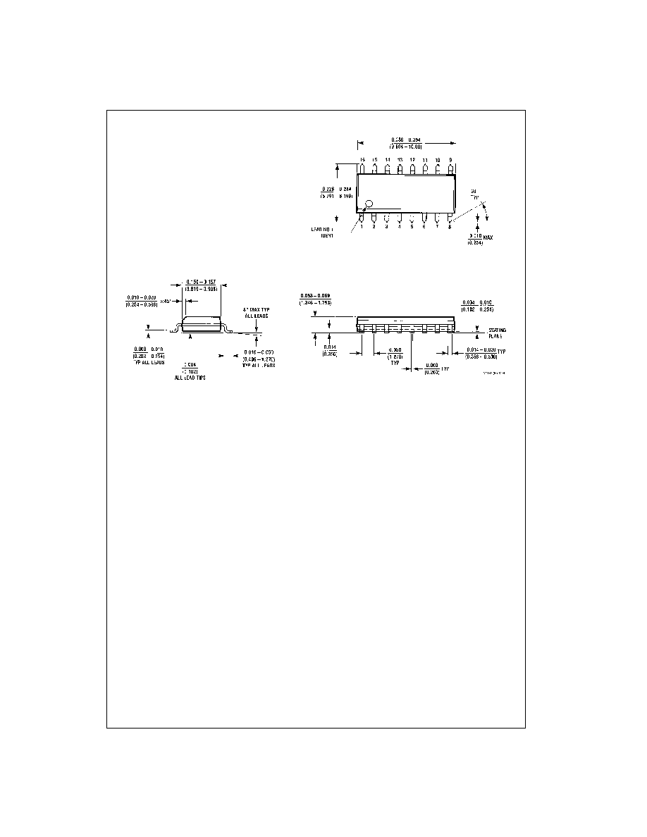
Physical Dimensions
inches (millimeters) unless otherwise noted
16-Lead Small Outline Integrated Circuit (SOIC), JEDEC MS-012, 0.150" Narrow Body
Package Number M16A