© 1999 Fairchild Semiconductor Corporation
DS009973
www.fairchildsemi.com
November 1988
Revised October 1999
74
A
C
57
3
∑ 74ACT573 O
c
t
a
l
Lat
ch w
i
th 3-
ST
A
T
E O
u
t
put
s
74AC573 ∑ 74ACT573
Octal Latch with 3-STATE Outputs
General Description
The 74AC573 and 74ACT573 are high-speed octal latches
with buffered common Latch Enable (LE) and buffered
common Output Enable (OE) inputs.
The 74AC573 and 74ACT573 are functionally identical to
the 74AC373 and 74ACT373 but with inputs and outputs
on opposite sides.
Features
s
I
CC
and I
OZ
reduced by 50%
s
Inputs and outputs on opposite sides of package allow-
ing easy interface with microprocessors
s
Useful as input or output port for microprocessors
s
Functionally identical to 74AC373 and 74ACT373
s
3-STATE outputs for bus interfacing
s
Outputs source/sink 24 mA
s
74ACT573 has TTL-compatible inputs
Ordering Code:
Device also available in Tape and Reel. Specify by appending suffix letter "X" to the ordering code.
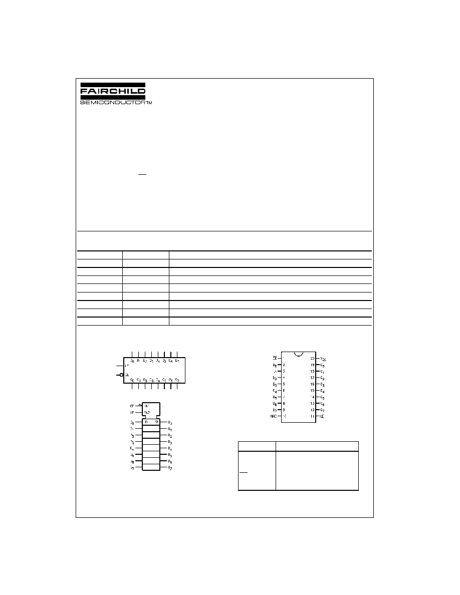
Logic Symbols
IEEE/IEC
Connection Diagram
Pin Descriptions
FACT
TM
is a trademark of Fairchild Semiconductor Corporation.
Order Number
Package Number
Package Description
74AC573SC
M20B
20-Lead Small Outline Integrated Circuit (SOIC), JEDEC MS--013, 0.300" Wide Body
74AC573SJ
M20D
20-Lead Small Outline Package (SOP), EIAJ TYPE II, 5.3mm Wide
74AC573MTC
MTC20
20-Lead Thin Shrink Small Outline Package (TSSOP), JEDEC MO-153, 4.4mm Wide
74AC573PC
N20A
20-Lead Plastic Dual-In-Line Package (PDIP), JEDEC MS-001, 0.300" Wide
74ACT573SC
M20B
20-Lead Small Outline Integrated Circuit (SOIC), JEDEC MS--013, 0.300" Wide Body
74ACT573SJ
M20D
20-Lead Small Outline Package (SOP), EIAJ TYPE II, 5.3mm Wide
74ACT573MTC
MTC20
20-Lead Thin Shrink Small Outline Package (TSSOP), JEDEC MO-153, 4.4mm Wide
74ACT573PC
N20A
20-Lead Plastic Dual-In-Line Package (PDIP), JEDEC MS-001, 0.300" Wide
Pin Names
Description
D
0
≠D
7
Data Inputs
LE
Latch Enable Input
OE
3-STATE Output Enable Input
O
0
≠O
7
3-STATE Latch Outputs
www.fairchildsemi.com
2
74AC573
∑ 74ACT573
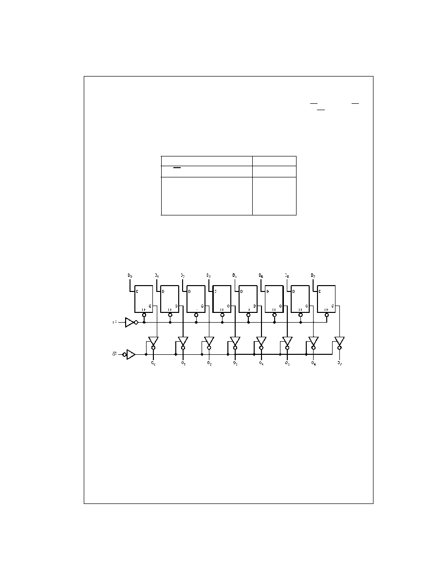
Functional Description
The 74AC573 and 74ACT573 contain eight D-type latches
with 3-STATE output buffers. When the Latch Enable (LE)
input is HIGH, data on the D
n
inputs enters the latches. In
this condition the latches are transparent, i.e., a latch out-
put will change state each time its D-type input changes.
When LE is LOW the latches store the information that was
present on the D-type inputs a setup time preceding the
HIGH-to-LOW transition of LE. The 3-STATE buffers are
controlled by the Output Enable (OE) input. When OE is
LOW, the buffers are enabled. When OE is HIGH the buff-
ers are in the high impedance mode but this does not inter-
fere with entering new data into the latches.
Truth Table
H
=
HIGH Voltage
L
=
LOW Voltage
Z
=
High Impedance
X
=
Immaterial
O
0
=
Previous O
0
before HIGH-to-LOW transition of Latch Enable
Logic Diagram
Please note that this diagram is provided only for the understanding of logic operations and should not be used to estimate propagation delays.
Inputs
Outputs
OE
LE
D
O
n
L
H
H
H
L
H
L
L
L
L
X
O
0
H
X
X
Z
3
www.fairchildsemi.com
74
A
C
57
3
∑ 74ACT573
Absolute Maximum Ratings
(Note 1)
Recommended Operating
Conditions
Note 1: Absolute maximum ratings are those values beyond which damage
to the device may occur. The databook specifications should be met, with-
out exception, to ensure that the system design is reliable over its power
supply, temperature, and output/input loading variables. Fairchild does not
recommend operation of FACT
TM
circuits outside databook specifications.
DC Electrical Characteristics for AC
Note 2: All outputs loaded; thresholds on input associated with output under test.
Note 3: I
IN
and I
CC
@ 3.0V are guaranteed to be less than or equal to the respective limit @ 5.5V V
CC
.
Note 4: Maximum test duration 2.0 ms, one output loaded at a time.
Supply Voltage (V
CC
)
-
0.5V to
+
7.0V
DC Input Diode Current (I
IK
)
V
I
=
-
0.5V
-
20 mA
V
I
=
V
CC
+
0.5V
+
20 mA
DC Input Voltage (V
I
)
-
0.5V to V
CC
+
0.5V
DC Output Diode Current (I
OK
)
V
O
=
-
0.5V
-
20 mA
V
O
=
V
CC
+
0.5V
+
20 mA
DC Output Voltage (V
O
)
-
0.5V to V
CC
+
0.5V
DC Output Source
or Sink Current (I
O
)
±
50 mA
DC V
CC
or Ground Current
per Output Pin (I
CC
or I
GND
)
±
50 mA
Storage Temperature (T
STG
)
-
65
∞
C to
+
150
∞
C
Junction Temperature (T
J
)
(PDIP)
140
∞
C
Supply Voltage (V
CC
)
AC
2.0V to 6.0V
ACT
4.5V to 5.5V
Input Voltage (V
I
)
0V to V
CC
Output Voltage (V
O
)
0V to V
CC
Operating Temperature (T
A
)
-
40
∞
C to
+
85
∞
C
Minimum Input Edge Rate (
V/
t)
AC Devices
V
IN
from 30% to 70% of V
CC
V
CC
@ 3.0V, 4.5V, 5.5V
125 mV/ns
ACT Devices
V
IN
from 0.8V to 2.0V
V
CC
@ 4.5V, 5.5V
125 mV/ns
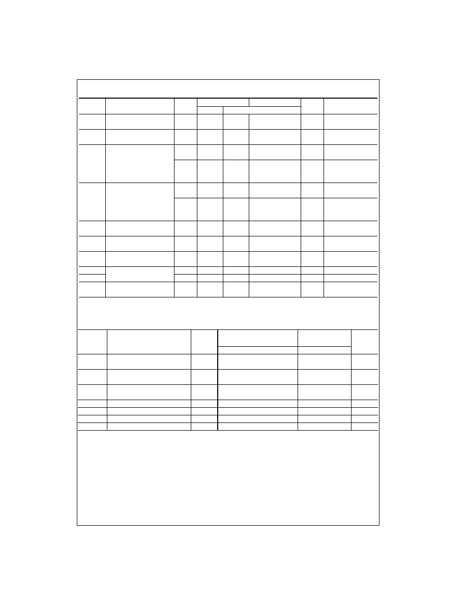
Symbol
Parameter
V
CC
T
A
=
+
25
∞
C
T
A
=
-
40
∞
C to
+
85
∞
C
Units
Conditions
(V)
Typ
Guaranteed Limits
V
IH
Minimum HIGH Level
3.0
1.5
2.1
2.1
V
V
OUT
=
0.1V
Input Voltage
4.5
2.25
3.15
3.15
or V
CC
-
0.1V
5.5
2.75
3.85
3.85
V
IL
Maximum LOW Level
3.0
1.5
0.9
0.9
V
V
OUT
=
0.1V
Input Voltage
4.5
2.25
1.35
1.35
or V
CC
-
0.1V
5.5
2.75
1.65
1.65
V
OH
Minimum HIGH Level
3.0
2.99
2.9
2.9
V
I
OUT
=
-
50
µ
A
Output Voltage
4.5
4.49
4.4
4.4
5.5
5.49
5.4
5.4
V
V
IN
=
V
IL
or V
IH
3.0
2.56
2.46
I
OH
=
-
12 mA
4.5
3.86
3.76
I
OH
=
-
24 mA
5.5
4.86
4.76
I
OH
=
-
24 mA (Note 2)
V
OL
Maximum LOW Level
3.0
0.002
0.1
0.1
V
I
OUT
=
50
µ
A
Output Voltage
4.5
0.001
0.1
0.1
5.5
0.001
0.1
0.1
V
V
IN
=
V
IL
or V
IH
3.0
0.36
0.44
I
OL
=
12 mA
4.5
0.36
0.44
I
OL
=
24 mA
5.5
0.36
0.44
I
OL
=
24 mA (Note 2)
I
IN
(Note 3)
Maximum Input Leakage Current
5.5
±
0.1
±
1.0
µ
A
V
I
=
V
CC
, GND
I
OLD
Minimum Dynamic
5.5
75
mA
V
OLD
=
1.65V Max
I
OHD
Output Current (Note 4)
5.5
-
75
mA
V
OHD
=
3.85V Min
I
CC
Maximum Quiescent
5.5
4.0
40.0
µ
A
V
IN
=
V
CC
or GND
(Note 3)
Supply Current
I
OZ
Maximum 3-STATE
5.5
±
0.25
±
2.5
µ
A
V
I
(OE)
=
V
IL
, V
IH
Leakage Current
V
I
=
V
CC
, GND
V
O
=
V
CC
, GND
www.fairchildsemi.com
4
74AC573
∑ 74ACT573
AC Electrical Characteristics for AC
Note 5: Voltage Range 5.0 is 5.0V
±
0.5V
Voltage Range 3.3 is 3.3V
±
0.3V
AC Operating Requirements for AC
Note 6: Voltage Range 5.0 is 5.0V
±
0.5V
Voltage Range 3.3 is 3.3V
±
0.3V
V
CC
T
A
=
+
25
∞
C
T
A
=
-
40
∞
C to
+
85
∞
C
Symbol
Parameter
(V)
C
L
=
50 pF
C
L
=
50 pF
Units
(Note 5)
Min
Typ
Max
Min
Max
t
PHL
Propagation Delay
3.3
0.5
8.5
10.5
2.5
11.0
ns
t
PLH
D
n
to O
n
5.0
1.5
5.5
7.0
1.5
7.5
t
PLH
Propagation Delay
3.3
2.5
8.5
12.0
2.5
12.5
ns
t
PHL
LE to O
n
5.0
2.0
6.0
8.0
2.0
8.5
t
PZL
Output Enable Time
3.3
2.5
8.5
13.0
2.5
13.5
ns
t
PZH
5.0
1.5
6.0
8.5
1.5
9.0
t
PHZ
Output Disable Time
3.3
1.0
9.0
14.5
1.0
15.0
ns
t
PLZ
5.0
1.0
6.0
9.5
1.0
10.0
V
CC
T
A
=
+
25
∞
C
T
A
=
-
40
∞
C to
+
85
∞
C
Symbol
Parameter
(V)
C
L
=
50 pF
C
L
=
50 pF
Units
(Note 6)
Typ
Guaranteed Minimum
t
S
Setup Time, HIGH or LOW
3.3
0
3.0
3.0
ns
D
n
to LE
5.0
0
3.0
3.0
t
H
Hold Time, HIGH or LOW
3.3
0
1.5
1.5
ns
D
n
to LE
5.0
0
1.5
1.5
t
W
LE Pulse Width, HIGH
3.3
2.0
4.0
4.0
ns
5.0
2.0
4.0
4.0
5
www.fairchildsemi.com
74
A
C
57
3
∑ 74ACT573
DC Electrical Characteristics for ACT
Note 7: All outputs loaded; thresholds on input associated with output under test.
Note 8: Maximum test duration 2.0 ms, one output loaded at a time.
AC Electrical Characteristics for ACT
Note 9: Voltage Range 5.0 is 5.0V
±
0.5V
Symbol
Parameter
V
CC
T
A
=
+
25
∞
C
T
A
=
-
40
∞
C to
+
85
∞
C
Units
Conditions
(V)
Typ
Guaranteed Limits
V
IH
Minimum HIGH Level
4.5
1.5
2.0
2.0
V
V
OUT
=
0.1V
Input Voltage
5.5
1.5
2.0
2.0
or V
CC
-
0.1V
V
IL
Maximum LOW Level
4.5
1.5
0.8
0.8
V
V
OUT
=
0.1V
Input Voltage
5.5
1.5
0.8
or V
CC
-
0.1V
V
OH
Minimum HIGH Level
4.5
4.49
4.4
4.4
V
I
OUT
=
-
50
µ
A
Output Voltage
5.5
5.49
5.4
5.4
V
IN
=
V
IL
or V
IH
4.5
3.86
3.76
V
I
OH
=
-
24 mA
5.5
4.86
4.76
I
OH
=
-
24 mA (Note 7)
V
OL
Maximum LOW Level
4.5
0.001
0.1
0.1
V
I
OUT
=
50
µ
A
Output Voltage
5.5
0.001
0.1
0.1
V
IN
=
V
IL
or V
IH
4.5
0.36
0.44
V
I
OL
=
24 mA
5.5
0.36
0.44
I
OL
=
24 mA (Note 7)
I
IN
Maximum Input
5.5
±
0.1
±
1.0
µ
A
V
I
=
V
CC
, GND
Leakage Current
I
OZ
Maximum 3-STATE
5.5
±
0.25
±
2.5
µ
A
V
I
=
V
IL
, V
IH
Leakage Current
V
O
=
V
CC
, GND
I
CCT
Maximum
5.5
0.6
1.5
mA
V
I
=
V
CC
-
2.1V
I
CC
/Input
I
OLD
Minimum Dynamic
5.5
75
mA
V
OLD
=
1.65V Max
I
OHD
Output Current (Note 8)
5.5
-
75
mA
V
OHD
=
3.85V Min
I
CC
Maximum Quiescent
5.5
4.0
40.0
µ
A
V
IN
=
V
CC
or GND
Supply Current
V
CC
T
A
=
+
25
∞
C
T
A
=
-
40
∞
C to
+
85
∞
C
Symbol
Parameter
(V)
C
L
=
50 pF
C
L
=
50 pF
Units
(Note 9)
Min
Typ
Max
Min
Max
t
PLH
Propagation Delay
5.0
2.5
6.0
10.5
2.0
12.0
ns
t
PHL
D
n
to O
n
t
PLH
Propagation Delay
5.0
3.0
6.0
10.5
2.5
12.0
ns
LE to O
n
t
PHL
Propagation Delay
5.0
2.5
5.5
9.5
2.0
10.5
ns
LE to O
n
t
PZH
Output Enable Time
5.0
2.0
5.5
10.0
1.5
11.0
ns
t
PZL
Output Enable Time
5.0
1.5
5.5
9.5
1.5
10.5
ns
t
PHZ
Output Disable Time
5.0
2.5
6.5
11.0
1.5
12.5
ns
t
PLZ
Output Disable Time
5.0
1.5
5.0
8.5
1.0
9.5
ns