 | –≠–ª–µ–∫—Ç—Ä–æ–Ω–Ω—ã–π –∫–æ–º–ø–æ–Ω–µ–Ω—Ç: 74ACT652 | –°–∫–∞—á–∞—Ç—å:  PDF PDF  ZIP ZIP |
© 2000 Fairchild Semiconductor Corporation
DS500310
www.fairchildsemi.com
August 1999
Revised September 2000
7
4
AC
T6
52 T
r
anscei
ver/
R
egis
ter
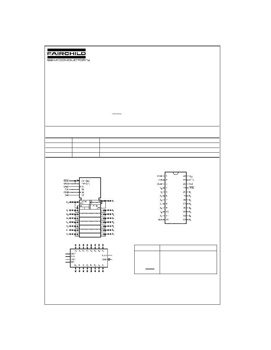
74ACT652
Transceiver/Register
General Description
The ACT652 consists of bus transceiver circuits with D-
type flip-flops, and control circuitry arranged for multiplexed
transmission of data directly from the input bus or from
internal registers. Data on the A or B bus will be clocked
into the registers as the appropriate clock pin goes to the
HIGH logic level. Output Enable pins (OEAB, OEBA) are
provided to control the transceiver function.
Features
s
Independent registers for A and B buses
s
Multiplexed real-time and stored data
s
Outputs source/sink 24 mA
s
TTL-compatible inputs
Ordering Code:
Device also available in Tape and Reel. Specify by appending suffix letter "X" to the ordering code.
Logic Symbols
IEEE/IEC
Connection Diagram
Pin Descriptions
FACT
is a trademark of Fairchild Semiconductor Corporation.
Order Number
Package Number
Package Description
74ACT652SC
M24B
24-Lead Small Outline Integrated Circuit (SOIC), JEDEC MS-013, 0.300 Wide
74ACT652MTC
MTC24
24-Lead Thin Shrink Small Outline Package (TSSOP), JEDEC MO-153, 4.4mm Wide
74ACT652SPC
N24C
24-Lead Plastic Dual-In-Line Package (PDIP), JEDEC MS-001, 0.300 Wide
Pin Names
Description
A
0
≠A
7
, B
0
≠B
7
A and B Inputs/3-STATE Outputs
CPAB, CPBA
Clock Inputs
SAB, SBA
Select Inputs
OEAB, OEBA
Output Enable Inputs
www.fairchildsemi.com
2
74ACT652
Function Table
H
=
HIGH Voltage Level
L
=
LOW Voltage Level
X
=
Immaterial
=
LOW-to-HIGH Clock Transition
Note 1: The data output functions may be enabled or disabled by various signals at OEAB or OEBA inputs. Data input functions are always enabled, i.e.,
data at the bus pins will be stored on every LOW-to-HIGH transition on the clock inputs.
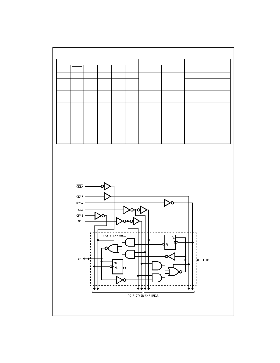
Logic Diagram
Please note that this diagram is provided only for the understanding of logic operations and should not be used to estimate propagation delays.
Inputs
Inputs/Outputs (Note 1)
Operating Mode
OEAB
OEBA
CPAB
CPBA
SAB
SBA
A
0
thru A
7
B
0
thru B
7
L
H
H or L
H or L
X
X
Input
Input
Isolation
L
H
X
X
Store A and B Data
X
H
H or L
X
X
Input
Not Specified
Store A, Hold B
H
H
X
X
Input
Output
Store A in Both Registers
L
X
H or L
X
X
Not Specified
Input
Hold A, Store B
L
L
X
X
Output
Input
Store B in Both Registers
L
L
X
X
X
L
Output
Input
Real-Time B Data to A Bus
L
L
X
H or L
X
H
Store B Data to A Bus
H
H
X
X
L
X
Input
Output
Real-Time A Data to B Bus
H
H
H or L
X
H
X
Stored A Data to B Bus
H
L
H or L
H or L
H
H
Output
Output
Stored A Data to B Bus and
Stored B Data to A Bus
3
www.fairchildsemi.com
74
A
C
T
6
5
2
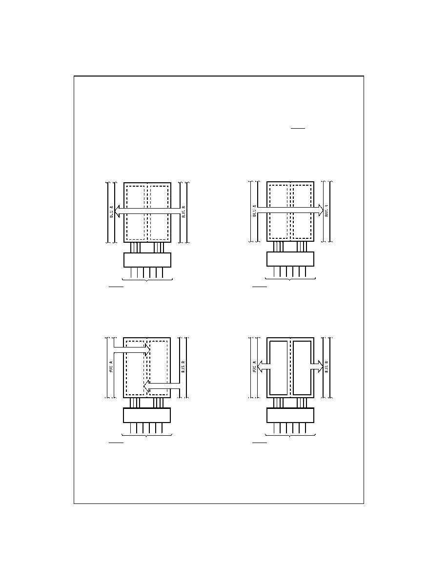
Functional Description
In the transceiver mode, data present at the HIGH imped-
ance port may be stored in either the A or B register or
both.
The select (SAB, SBA) controls can multiplex stored and
real-time.
The examples in Figure 1 demonstrate the four fundamen-
tal bus-management functions that can be performed with
the Octal bus transceivers and receivers.
Data on the A or B data bus, or both can be stored in the
internal D-type flip-flop by LOW to HIGH transitions at the
appropriate Clock Inputs (CPAB, CPBA) regardless of the
Select or Output Enable Inputs. When SAB and SBA are in
the real time transfer mode, it is also possible to store data
without using the internal D-type flip-flops by simulta-
neously enabling OEAB and OEBA. In this configuration
each Output reinforces its Input. Thus when all other data
sources to the two sets of bus lines are in a HIGH imped-
ance state, each set of bus lines will remain at its last state.
FIGURE 1.
Note A: Real-Time
Note B: Real-Time
Transfer Bus B to Bus A
Transfer Bus A to Bus B
OEAB
OEBA
CPAB
CPBA
SAB
SBA
OEAB
OEBA
CPAB
CPBA
SAB
SBA
L
L
X
X
X
L
H
H
X
X
L
X
Note C: Storage
Note D: Transfer Storage
Data to A or B
OEAB
OEBA
CPAB
CPBA
SAB
SBA
OEAB
OEBA
CPAB
CPBA
SAB
SBA
X
H
X
X
X
H
L
H or L
H or L
H
H
L
X
X
X
X
L
H
X
X
www.fairchildsemi.com
4
74ACT652
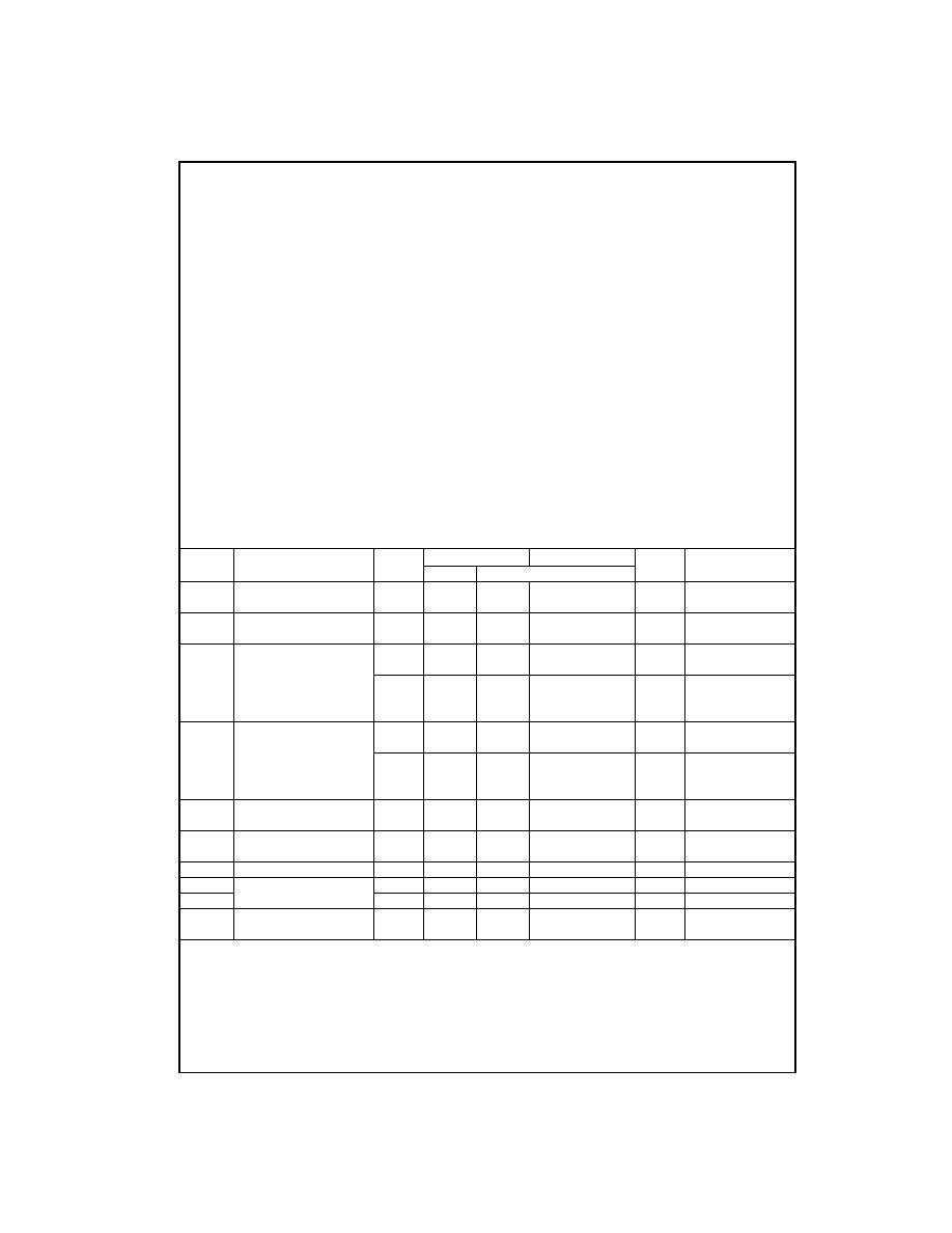
Absolute Maximum Ratings
(Note 2)
Recommended Operating
Conditions
Note 2: Absolute maximum ratings are those values beyond which damage
to the device may occur. The databook specifications should be met, with-
out exception, to ensure that the system design is reliable over its power
supply, temperature, and output/input loading variables. Fairchild does not
recommend operation of FACT
circuits outside databook specifications.
DC Electrical Characteristics
Note 3: All outputs loaded; thresholds on input associated with output under test.
Note 4: Maximum test duration 2.0 ms, one output loaded at a time.
Supply Voltage (V
CC
)
-
0.5V to
+
7.0V
DC Input Diode Current (I
IK
)
V
I
=
-
0.5V
-
20 mA
V
I
=
V
CC
+
0.5V
+
20 mA
DC Input Voltage (V
I
)
-
0.5V to V
CC
+
0.5V
DC Output Diode Current (I
OK
)
V
O
=
-
0.5V
-
20 mA
V
O
=
V
CC
+
0.5V
+
20 mA
DC Output Voltage (V
O
)
-
0.5V to V
CC
+
0.5V
DC Output Source
or Sink Current (I
O
)
±
50 mA
DC V
CC
or Ground Current
per Output Pin (I
CC
or I
GND
)
±
50 mA
Storage Temperature (T
STG
)
-
65
∞
C to
+
150
∞
C
DC Latch-Up Source
or Sink Current
±
300 mA
Junction Temperature (T
J
)
PDIP
140
∞
C
Supply Voltage (V
CC
)
4.5V to 5.5V
Input Voltage (V
I
)
0V to V
CC
Output Voltage (V
O
)
0V to V
CC
Operating Temperature (T
A
)
-
40
∞
C to
+
85
∞
C
Minimum Input Edge Rate
V/
t
V
IN
from 0.8V to 2.0V
V
CC
@ 4.5V, 5.5V
125 mV/ns
Symbol
Parameter
V
CC
T
A
=
+
25
∞
C
T
A
=
-
40
∞
C to
+
85
∞
C
Units
Conditions
(V)
Typ
Guaranteed Limits
V
IH
Minimum HIGH Level
4.5
1.5
2.0
2.0
V
V
OUT
=
0.1V
Input Voltage
5.5
1.5
2.0
2.0
or V
CC
-
0.1V
V
IL
Maximum LOW Level
4.5
1.5
0.8
0.8
V
V
OUT
=
0.1V
Input Voltage
5.5
1.5
0.8
0.8
or V
CC
-
0.1V
V
OH
Minimum HIGH Level
4.5
4.49
4.4
4.4
V
I
OUT
=
-
50
µ
A
Output Voltage
5.5
5.49
5.4
5.4
V
IN
=
V
IL
or V
IH
4.5
3.86
3.76
V
I
OH
=
-
24 mA
5.5
4.86
4.76
I
OH
=
-
24 mA (Note 3)
V
OL
Maximum LOW Level
4.5
0.001
0.1
0.1
V
I
OUT
=
50
µ
A
Output Voltage
5.5
0.001
0.1
0.1
V
IN
=
V
IL
or V
IH
4.5
0.36
0.44
V
I
OL
=
24 mA
5.5
0.36
0.44
I
OL
=
24 mA (Note 3)
I
IN
Maximum Input
5.5
±
0.1
±
1.0
µ
A
V
I
=
V
CC
, GND
Leakage Current
I
OZT
Maximum I/O
5.5
±
0.6
±
6.0
µ
A
V
I
=
V
IL
, V
IH
Leakage Current
V
O
=
V
CC
, GND
I
CCT
Maximum I
CC
/Input
5.5
0.6
1.5
mA
V
I
=
V
CC
-
2.1V
I
OLD
Minimum Dynamic
5.5
75
mA
V
OLD
=
1.65V Max
I
OHD
Output Current (Note 4)
5.5
-
75
mA
V
OHD
=
3.85V Min
I
CC
Maximum Quiescent
5.5
8.0
80.0
µ
A
V
IN
=
V
CC
or GND
Supply Current

5
www.fairchildsemi.com
74
A
C
T
6
5
2
AC Electrical Characteristics
Note 5: Voltage Range 5.0 is 5.0V
±
0.5V.
Capacitance
V
CC
T
A
=
+
25
∞
C
T
A
=
-
40
∞
C to
+
85
∞
C
Symbol
Parameter
(V)
C
L
=
50 pF
C
L
=
50 pF
Units
(Note 5)
Min
Typ
Max
Min
Max
f
MAX
Max. Clock Frequency
5.0
MHz
t
PLH
Propagation Delay
5.0
2.0
7.0
9.5
2.0
10.0
ns
t
PHL
Clock to Bus
t
PLH
Propagation Delay
5.0
2.0
6.5
9.0
2.0
9.5
ns
t
PHL
Bus to Bus
t
PLH
Propagation Delay
5.0
2.5
6.5
10.0
2.5
10.5
ns
t
PHL
SBA or SAB to A or B
t
PZH
Enable Time
5.0
2.0
7.0
10.5
2.0
11.0
ns
t
PZL
OEBA to A (Note 5)
t
PHZ
Disable Time
5.0
1.0
5.0
8.0
1.0
8.5
t
PLZ
OEBA to A (Note 5)
t
PZH
Enable Time
5.0
2.0
7.0
10.5
2.0
11.0
t
PZL
OEAB to B
t
PHZ
Disable Time
5.0
1.0
5.0
8.0
1.0
8.5
ns
t
PLZ
OEAB to B
t
s
(H)
Setup Time, HIGH or
5.0
3.0
3.0
ns
t
s
(L)
LOW, Bus to Clock
t
h
(H)
Hold Time, HIGH or
5.0
1.5
1.5
ns
t
h
(L)
LOW, Bus to Clock
t
w
(H)
Clock Pulse Width
5.0
4.0
4.0
ns
t
w
(L)
HIGH or LOW
Symbol
Parameter
Typ
Units
Conditions
C
IN
Input Capacitance
4.5
pF
V
CC
=
5.0V
C
PD
Power Dissipation Capacitance
54
pF
V
CC
=
5.0V