 | –≠–ª–µ–∫—Ç—Ä–æ–Ω–Ω—ã–π –∫–æ–º–ø–æ–Ω–µ–Ω—Ç: 74ACT74PC | –°–∫–∞—á–∞—Ç—å:  PDF PDF  ZIP ZIP |
© 1999 Fairchild Semiconductor Corporation
DS009920
www.fairchildsemi.com
November 1988
Revised November 1999
7
4
AC
7
4
∑ 74ACT74
Dual
D
-
T
y
pe Posit
i
ve Edge-
T
ri
ggered Fl
ip-
F
lop
74AC74 ∑ 74ACT74
Dual D-Type Positive Edge-Triggered Flip-Flop
General Description
The AC/ACT74 is a dual D-type flip-flop with Asynchronous
Clear and Set inputs and complementary (Q, Q) outputs.
Information at the input is transferred to the outputs on the
positive edge of the clock pulse. Clock triggering occurs at
a voltage level of the clock pulse and is not directly related
to the transition time of the positive-going pulse. After the
Clock Pulse input threshold voltage has been passed, the
Data input is locked out and information present will not be
transferred to the outputs until the next rising edge of the
Clock Pulse input.
Asynchronous Inputs:
LOW input to S
D
(Set) sets Q to HIGH level
LOW input to C
D
(Clear) sets Q to LOW level
Clear and Set are independent of clock
Simultaneous LOW on C
D
and S
D
makes both Q and Q
HIGH
Features
s
I
CC
reduced by 50%
s
Output source/sink 24 mA
s
ACT74 has TTL-compatible inputs
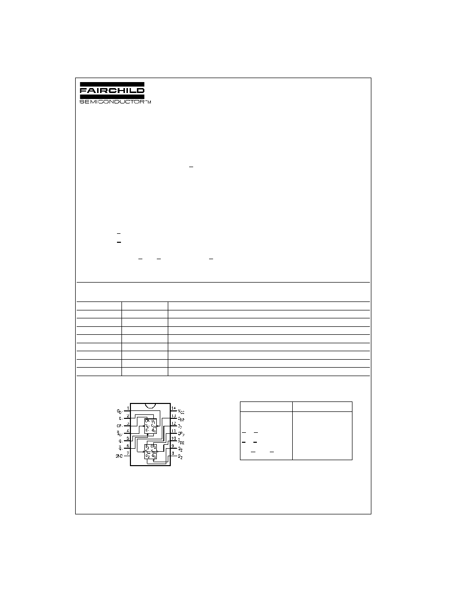
Ordering Code:
Device also available in Tape and Reel. Specify by appending suffix letter "X" to the ordering code.
Connection Diagram
Pin Descriptions
FACT
is a trademark of Fairchild Semiconductor Corporation.
Order Number
Package Number
Package Description
74AC74SC
M14A
14-Lead Small Outline Integrated Circuit (SOIC), JEDEC MS-120, 0.150" Narrow Body
74AC74SJ
M14D
14-Lead Small Outline Package (SOP), EIAJ TYPE II, 5.3mm Wide
74AC74MTC
MTC14
14-Lead Thin Shrink Small Outline Package (TSSOP), JEDEC MO-153, 4.4mm Wide
74AC74PC
N14A
14-Lead Plastic Dual-In-Line Package (PDIP), JEDEC MS-001, 0.300" Wide
74ACT74SC
M14A
14-Lead Small Outline Integrated Circuit (SOIC), JEDEC MS-120, 0.150" Narrow Body
74ACT74SJ
M14D
14-Lead Small Outline Package (SOP), EIAJ TYPE II, 5.3mm Wide
74ACT74MTC
MTC14
14-Lead Thin Shrink Small Outline Package (TSSOP), JEDEC MO-153, 4.4mm Wide
74ACT74PC
N14A
14-Lead Plastic Dual-In-Line Package (PDIP), JEDEC MS-001, 0.300" Wide
Pin Names
Description
D
1
, D
2
Data Inputs
CP
1
, CP
2
Clock Pulse Inputs
C
D1
, C
D2
Direct Clear Inputs
S
D1
, S
D2
Direct Set Inputs
Q
1
, Q
1
, Q
2
, Q
2
Outputs
www.fairchildsemi.com
2
74AC74
∑
74
A
C
T74
Logic Symbols
IEEE/IEC
Truth Table
(Each Half)
H
=
HIGH Voltage Level
L
=
LOW Voltage Level
X
=
Immaterial
=
LOW-to-HIGH Clock Transition
Q
0
(Q
0
)
=
Previous Q (Q) before LOW-to-HIGH Transition of Clock
Logic Diagram
Please note that this diagram is provided only for the understanding of logic operations and should not be used to estimate propagation delays.
Inputs
Outputs
S
D
C
D
CP
D
Q
Q
L
H
X
X
H
L
H
L
X
X
L
H
L
L
X
X
H
H
H
H
H
H
L
H
H
L
L
H
H
H
L
X
Q
0
Q
0
3
www.fairchildsemi.com
74
A
C
74
∑
74ACT74
Absolute Maximum Ratings
(Note 1)
Recommended Operating
Conditions
Note 1: Absolute maximum ratings are those values beyond which damage
to the device may occur. The databook specifications should be met, with-
out exception, to ensure that the system design is reliable over its power
supply, temperature, and output/input loading variables. Fairchild does not
recommend operation of FACT
circuits outside databook specifications.
DC Electrical Characteristics for AC
Note 2: All outputs loaded; thresholds on input associated with output under test.
Note 3: Maximum test duration 2.0 ms, one output loaded at a time.
Note 4: I
IN
and I
CC
@ 3.0V are guaranteed to be less than or equal to the respective limit @ 5.5V V
CC
.
Supply Voltage (V
CC
)
-
0.5V to
+
7.0V
DC Input Diode Current (I
IK
)
V
I
=
-
0.5V
-
20 mA
V
I
=
V
CC
+
0.5V
+
20 mA
DC Input Voltage (V
I
)
-
0.5V to V
CC
+
0.5V
DC Output Diode Current (I
OK
)
V
O
=
-
0.5V
-
20 mA
V
O
=
V
CC
+
0.5V
+
20 mA
DC Output Voltage (V
O
)
-
0.5V to V
CC
+
0.5V
DC Output Source
or Sink Current (I
O
)
±
50 mA
DC V
CC
or Ground Current
per Output Pin (I
CC
or I
GND
)
±
50 mA
Storage Temperature (T
STG
)
-
65
∞
C to
+
150
∞
C
Junction Temperature (T
J
)
PDIP
140
∞
C
Supply Voltage (V
CC
)
AC
2.0V to 6.0V
ACT
4.5V to 5.5V
Input Voltage (V
I
)
0V to V
CC
Output Voltage (V
O
)
0V to V
CC
Operating Temperature (T
A
)
-
40
∞
C to
+
85
∞
C
Minimum Input Edge Rate (
V/
t)
AC Devices
V
IN
from 30% to 70% of V
CC
V
CC
@ 3.3V, 4.5V, 5.5V
125 mV/ns
Minimum Input Edge Rate (
V/
t)
ACT Devices
V
IN
from 0.8V to 2.0V
V
CC
@ 4.5V, 5.5V
125 mV/ns
Symbol
Parameter
V
CC
T
A
=
+
25
∞
C
T
A
=
-
40
∞
C to
+
85
∞
C
Units
Conditions
(V)
Typ
Guaranteed Limits
V
IH
Minimum HIGH
3.0
1.5
2.1
2.1
V
OUT
=
0.1V
Level Input
4.5
2.25
3.15
3.15
V
or V
CC
-
0.1V
Voltage
5.5
2.75
3.85
3.85
V
IL
Maximum LOW
3.0
1.5
0.9
0.9
V
OUT
=
0.1V
Level Input
4.5
2.25
1.35
1.35
V
or V
CC
-
0.1V
Voltage
5.5
2.75
1.65
1.65
V
OH
Minimum HIGH
3.0
2.99
2.9
2.9
Level Output
4.5
4.49
4.4
4.4
V
I
OUT
=
-
50
µ
A
Voltage
5.5
5.49
5.4
5.4
V
IN
=
V
IL
or V
IH
3.0
2.56
2.46
I
OH
=
-
12 mA
4.5
3.86
3.76
V
I
OH
=
-
24 m
5.5
4.86
4.76
I
OH
=
-
24 m (Note 2)
V
OL
Maximum LOW
3.0
0.002
0.1
0.1
Level Output
4.5
0.001
0.1
0.1
V
I
OUT
=
50
µ
A
Voltage
5.5
0.001
0.1
0.1
V
IN
=
V
IL
or V
IH
3.0
0.36
0.44
I
OL
=
12 mA
4.5
0.36
0.44
V
I
OL
=
24 mA
5.5
0.36
0.44
I
OL
=
24 mA (Note 2)
I
IN
(Note 4)
Maximum InputLeakage Current
5.5
±
0.1
±
1.0
µ
A
V
I
=
V
CC
, GND
I
OLD
Minimum Dynamic
5.5
75
mA
V
OLD
=
1.65V Max
I
OHD
Output Current (Note 3)
5.5
-
75
mA
V
OHD
=
3.85V Min
I
CC
Maximum Quiescent
5.5
2.0
20.0
µ
A
V
IN
=
V
CC
(Note 4)
Supply Current
or GND
www.fairchildsemi.com
4
74AC74
∑
74
A
C
T74
DC Electrical Characteristics for ACT
Note 5: All outputs loaded; thresholds on input associated with output under test.
Note 6: Maximum test duration 2.0 ms, one output loaded at a time.
AC Electrical Characteristics for AC
Note 7: Voltage Range 3.3 is 3.3V
±
0.3V
Voltage Range 5.0 is 5.0V
±
0.5V
Symbol
Parameter
V
CC
T
A
=
+
25
∞
C
T
A
=
-
40
∞
C to
+
85
∞
C
Units
Conditions
(V)
Typ
Guaranteed Limits
V
IH
Minimum HIGH Level
4.5
1.5
2.0
2.0
V
V
OUT
=
0.1V
Input Voltage
5.5
1.5
2.0
2.0
or V
CC
-
0.1V
V
IL
Maximum LOW Level
4.5
1.5
0.8
0.8
V
V
OUT
=
0.1V
Output Voltage
5.5
1.5
0.8
0.8
or V
CC
-
0.1V
V
OH
Minimum HIGH Level
4.5
4.49
4.4
4.4
V
I
OUT
=
-
50
µ
A
Output Voltage
5.5
5.49
5.4
5.4
V
IN
=
V
IL
or V
IH
4.5
3.86
3.76
V
I
OH
=
-
24 mA
5.5
4.86
4.76
I
OH
=
-
24 mA (Note 5)
V
OL
Maximum LOW Level
4.5
0.001
0.1
0.1
V
I
OUT
=
50
µ
A
Output Voltage
5.5
0.001
0.1
0.1
V
IN
=
V
IL
or V
IH
4.5
0.36
0.44
V
I
OL
=
24 mA
5.5
0.36
0.44
I
OL
=
24 mA (Note 5)
I
IN
Maximum Input
5.5
±
0.1
±
1.0
µ
A
V
I
=
V
CC
, GND
Leakage Current
I
CCT
Maximum
5.5
0.6
1.5
mA
V
I
=
V
CC
-
2.1V
I
CC
/Input
I
OLD
Minimum Dynamic
5.5
75
mA
V
OLD
=
1.65V Max
I
OHD
Output Current (Note 6)
5.5
-
75
mA
V
OHD
=
3.85V Min
I
CC
Maximum Quiescent
5.5
2.0
20.0
µ
A
V
IN
=
V
CC
Supply Current
or GND
V
CC
T
A
=
+
25
∞
C
T
A
=
-
40
∞
C to
+
85
∞
C
Symbol
Parameter
(V)
C
L
=
50 pF
C
L
=
50 pF
Units
(Note 7)
Min
Typ
Max
Min
Max
f
MAX
Maximum Clock
3.3
100
125
95
MHz
Frequency
5.0
140
160
125
t
PLH
Propagation Delay
3.3
3.5
8.0
12.0
2.5
13.0
ns
C
Dn
or S
Dn
to Q
n
or Q
n
5.0
2.5
6.0
9.0
2.0
10.0
t
PHL
Propagation Delay
3.3
4.0
10.5
12.0
3.5
13.5
ns
C
Dn
or S
Dn
to Q
n
or Q
n
5.0
3.0
8.0
9.5
2.5
10.5
t
PLH
Propagation Delay
3.3
4.5
8.0
13.5
4.0
16.0
ns
CP
n
to Q
n
or Q
n
5.0
3.5
6.0
10.0
3.0
10.5
t
PHL
Propagation Delay
3.3
3.5
8.0
14.0
3.5
14.5
ns
CP
n
to Q
n
or Q
n
5.0
2.5
6.0
10.0
2.5
10.5

5
www.fairchildsemi.com
74
A
C
74
∑
74ACT74
AC Operating Requirements for AC
Note 8: Voltage Range 3.3 is 3.3V
±
0.3V
Voltage Range 5.0 is 5.0V
±
0.5V
AC Electrical Characteristics for ACT
Note 9: Voltage Range 5.0 is 5.0V
±
0.5V
AC Operating Requirements for ACT
Note 10: Voltage Range 5.0 is 5.0V
±
0.5V
Capacitance
V
CC
T
A
=
+
25
∞
C
T
A
=
-
40
∞
C to
+
85
∞
C
Symbol
Parameter
(V)
C
L
=
50 pF
C
L
=
50 pF
Units
(Note 8)
Typ
Guaranteed Minimum
t
S
Set-up Time, HIGH or LOW
3.3
1.5
4.0
4.5
ns
D
n
to CP
n
5.0
1.0
3.0
3.0
t
H
Hold Time, HIGH or LOW
3.3
-
2.0
0.5
0.5
ns
D
n
to CP
n
5.0
-
1.5
0.5
0.5
t
W
CP
n
or C
Dn
or S
Dn
3.3
3.0
5.5
7.0
ns
Pulse Width
5.0
2.5
4.5
5.0
t
rec
Recovery Time
3.3
-
2.5
0
0
ns
C
Dn
or S
Dn
to CP
5.0
-
2.0
0
0
V
CC
T
A
=
+
25
∞
C
T
A
=
-
40
∞
C to
+
85
∞
C
Symbol
Parameter
(V)
C
L
=
50 pF
C
L
=
50 pF
Units
(Note 9)
Min
Typ
Max
Min
Max
f
MAX
Maximum Clock
5.0
145
210
125
MHz
Frequency
t
PLH
Propagation Delay
5.0
3.0
5.5
9.5
2.5
10.5
ns
C
Dn
or S
Dn
to Q
n
or Q
n
t
PHL
Propagation Delay
5.0
3.0
6.0
10.0
3.0
11.5
ns
C
Dn
or S
Dn
to Q
n
or Q
n
t
PLH
Propagation Delay
5.0
4.0
7.5
11.0
4.0
13.0.
ns
CP
n
to Q
n
or Q
n
t
PHL
Propagation Delay
5.0
3.5
6.0
10.0
3.0
11.5
ns
CP
n
to Q
n
or Q
n
V
CC
T
A
=
+
25
∞
C
T
A
=
-
40
∞
C to
+
85
∞
C
Symbol
Parameter
(V)
C
L
=
50 pF
C
L
=
50 pF
Units
(Note 10)
Typ
Guaranteed Minimum
t
S
Set-up Time, HIGH or LOW
5.0
1.0
3.0
3.5
ns
D
n
to CP
n
t
H
Hold Time, HIGH or LOW
5.0
-
0.5
1.0
1.0
ns
D
n
to CP
n
t
W
CP
n
or C
Dn
or S
Dn
5.0
3.0
5.0
6.0
ns
Pulse Width
t
rec
Recovery Time
5.0
-
2.5
0
0
ns
C
Dn
or S
Dn
to CP
Symbol
Parameter
Typ
Units
Conditions
C
IN
Input Capacitance
4.5
pF
V
CC
=
OPEN
C
PD
Power Dissipation Capacitance
35.0
pF
V
CC
=
5.0V