Äîêóìåíòàöèÿ è îïèñàíèÿ www.docs.chipfind.ru
© 2000 Fairchild Semiconductor Corporation
DS009895
www.fairchildsemi.com
July 1988
Revised September 2000
7
4
AC
T8
25 8-
Bit
D-
T
y
pe F
l
i
p
-Fl
o
p
74ACT825
8-Bit D-Type Flip-Flop
General Description
The ACT825 is an 8-bit buffered register. They have Clock
Enable and Clear features which are ideal for parity bus
interfacing in high performance microprogramming sys-
tems. Also included are multiple enables that allow multi-
use control of the interface. The ACT825 has noninverting
outputs.
Features
s
Outputs source/sink 24 mA
s
Inputs and outputs are on opposite sides
s
TTL compatible inputs
Ordering Code:
Device also available in Tape and Reel. Specify by appending suffix letter "X" to the ordering code.
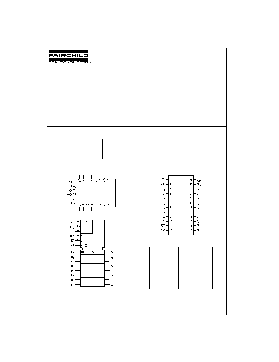
Logic Symbols
IEEE/IEC
Connection Diagram
Pin Descriptions
FACT
is a trademark of Fairchild Semiconductor.
Order Number
Package Number
Package Description
74ACT825SC
M24B
24-Lead Small Outline Integrated Circuit (SOIC), JEDEC MS-013, 0.300 Wide
74ACT825MTC
MTC24
24-Lead Thin Shrink Small Outline Package (TSSOP), JEDEC MO-153, 4.4mm Wide
74ACT825SPC
N24C
24-Lead Plastic Dual-In-Line Package (PDIP), JEDEC MS-001, 0.300 Wide
Pin Names
Description
D
0
D
7
Data Inputs
O
0
O
7
Data Outputs
OE
1
, OE
2
, OE
3
Output Enables
EN
Clock Enable
CLR
Clear
CP
Clock Input
www.fairchildsemi.com
2
74ACT825
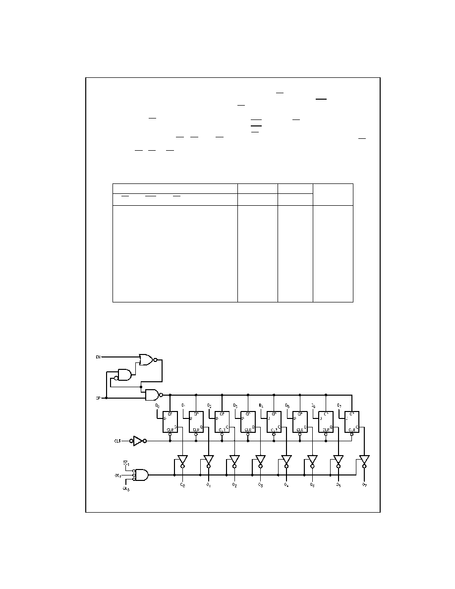
Functional Description
The ACT825 consists of eight D-type edge-triggered flip-
flops. These devices have 3-STATE outputs for bus sys-
tems, organized in a broadside pinning. In addition to the
clock and output enable pins, the buffered clock (CP) and
buffered Output Enable (OE) are common to all flip-flops.
The flip-flops will store the state of their individual D inputs
that meet the setup and hold time requirements on the
LOW-to-HIGH CP transition. With OE
1
, OE
2
and OE
3
LOW, the contents of the flip-flops are available at the out-
puts. When one of OE
1
, OE
2
or OE
3
is HIGH, the outputs
go to the high impedance state.
Operation of the OE input does not affect the state of the
flip-flops. The ACT825 has Clear (CLR) and Clock Enable
(EN) pins. These pins are ideal for parity bus interfacing in
high performance systems.
When CLR is LOW and OE is LOW, the outputs are LOW.
When CLR is HIGH, data can be entered into the flip-flops.
When EN is LOW, data on the inputs is transferred to the
outputs on the LOW-to-HIGH clock transition. When EN is
HIGH, the outputs do not change state, regardless of the
data or clock input transitions.
Function Table
H
=
HIGH Voltage Level
L
=
LOW Voltage Level
X
=
Immaterial
Z
=
High Impedance
=
LOW-to-HIGH Transition
NC
=
No Change
Logic Diagram
Please note that this diagram is provided only for the understanding of logic operations and should not be used to estimate propagation delays.
Inputs
Internal
Output
Function
OE
CLR
EN
CP
D
n
Q
O
H
X
L
L
L
Z
High-Z
H
X
L
H
H
Z
High-Z
H
L
X
X
X
L
Z
Clear
L
L
X
X
X
L
L
Clear
H
H
H
X
X
NC
Z
Hold
L
H
H
X
X
NC
NC
Hold
H
H
L
L
L
Z
Load
H
H
L
H
H
Z
Load
L
H
L
L
L
L
Load
L
H
L
H
H
H
Load
3
www.fairchildsemi.com
74
A
C
T
8
2
5
Absolute Maximum Ratings
(Note 1)
Recommended Operating
Conditions
Note 1: Absolute maximum ratings are those values beyond which damage
to the device may occur. The databook specifications should be met, with-
out exception, to ensure that the system design is reliable over its power
supply, temperature, and output/input loading variables. Fairchild does not
recommend operation of FACT
circuits outside databook specifications.
DC Electrical Characteristics
Note 2: All outputs loaded; thresholds on input associated with output under test.
Note 3: Maximum test duration 2.0 ms, one output loaded at a time.
Supply Voltage (V
CC
)
-
0.5V to 7.0V
DC Input Diode Current (I
IK
)
V
I
=
-
0.5V
-
20 mA
V
I
=
V
CC
+
0.5V
+
20 mA
DC Input Voltage (V
I
)
-
0.5V to V
CC
+
0.5V
DC Output Diode Current (I
OK
)
V
O
=
-
0.5V
-
20 mA
V
O
=
V
CC
+
0.5V
+
20 mA
DC Output Voltage (V
O
)
+
0.5V
DC Output Source or Sink Current
(I
O
)
±
50 mA
DC V
CC
or Ground Current
Per Output Pin (I
CC
or I
GND
)
±
50 mA
Storage Temperature (T
STG
)
-
65
°
C to
+
150
°
C
Junction Temperature (T
J
)
PDIP
140
°
C
Supply Voltage (V
CC
)
4.5V to 5.5V
Input Voltage (V
I
)
0V to V
CC
Output Voltage (V
O
)
0V to V
CC
Operating Temperature (T
A
)
-
40
°
C to
+
85
°
C
Minimum Input Edge Rate (
V/
t)
125 mV/ns
V
IN
from 0.8V to 2.0V
V
CC
@ 4.5V, 5.5V
Symbol
Parameter
V
CC
T
A
=
25
°
C
T
A
=
-
40
°
C to
+
85
°
C
Units
Conditions
(V)
Typ
Guaranteed Limits
V
IH
Minimum HIGH Level
4.5
1.5
2.0
2.0
V
V
OUT
=
0.1V
Input Voltage
5.5
1.5
2.0
2.0
or V
CC
-
0.1V
V
IL
Maximum LOW Level
4.5
1.5
0.8
0.8
V
V
OUT
=
0.1V
Input Voltage
5.5
1.5
0.8
0.8
or V
CC
-
0.1V
V
OH
Minimum HIGH Level
4.5
4.49
4.4
4.4
V
I
OUT
=
-
50
µ
A
Output Voltage
5.5
5.49
5.4
5.4
V
IN
=
V
IL
or V
IH
4.5
3.86
3.76
V
I
OH
=
-
24 mA
5.5
4.86
4.76
I
OH
=
-
24 mA (Note 2)
V
OL
Maximum LOW Level
4.5
0.001
0.1
0.1
V
I
OUT
=
50
µ
A
Output Voltage
5.5
0.001
0.1
0.1
V
IN
=
V
IL
or V
IH
4.5
0.36
0.44
V
I
OL
=
24 mA
5.5
0.36
0.44
I
OL
=
24 mA (Note 2)
I
IN
Maximum Input Leakage Current
5.5
±
0.1
±
1.0
µ
A
V
I
=
V
CC
, GND
I
OZ
Maximum
5.5
±
0.5
±
5.0
µ
A
V
I
=
V
IL
, V
IH
3-STATE Current
V
O
=
V
CC
, GND
I
CCT
Maximum I
CC
/Input
5.5
0.6
1.5
mA
V
I
=
V
CC
-
2.1V
I
OLD
Minimum Dynamic
5.5
75
mA
V
OLD
=
1.65V Max
I
OHD
Output Current (Note 3)
5.5
-
75
mA
V
OHD
=
3.85V Min
I
CC
Maximum Quiescent
5.5
8.0
80
µ
A
V
IN
=
V
CC
or GND
Supply Current
www.fairchildsemi.com
4
74ACT825
AC Electrical Characteristics
Note 4: Voltage Range 5.0 is 5.0V
±
0.5V
AC Operating Requirements
Note 5: Voltage Range 5.0 is 5.0V
±
0.5V
Capacitance
V
CC
T
A
=
+
25
°
C
T
A
=
-
40
°
C to
+
85
°
C
Symbol
Parameter
(V)
C
L
=
50 pF
C
L
=
50 pF
Units
(Note 4)
Min
Typ
Max
Min
Max
f
MAX
Maximum Clock
5.0
120
158
109
MHz
Frequency
t
PLH
Propagation Delay
5.0
1.5
5.5
9.5
1.5
10.5
ns
CP to O
n
t
PHL
Propagation Delay
5.0
2.0
5.5
9.5
1.5
10.5
ns
CP to O
n
t
PHL
Propagation Delay
5.0
2.5
8.0
13.5
2.0
15.5
ns
CLR to O
n
t
PZH
Output Enable Time
5.0
1.5
6.0
10.5
1.5
11.5
ns
OE to O
n
t
PZL
Output Enable Time
5.0
2.0
6.5
11.0
1.5
12.0
ns
OE to O
n
t
PHZ
Output Disable Time
5.0
1.5
6.5
11.0
1.5
12.0
ns
OE to O
n
t
PLZ
Output Disable Time
5.0
1.5
6.0
10.5
1.5
11.5
ns
OE to O
n
V
CC
T
A
=
+
25
°
C
T
A
=
-
40
°
C to
+
85
°
C
Symbol
Parameter
(V)
C
L
=
50 pF
C
L
=
50 pF
Units
(Note 5)
Typ
Guaranteed Minimum
t
S
Setup Time, HIGH or LOW
5.0
0.5
2.5
2.5
ns
D
n
to CP
t
H
Hold Time, HIGH or LOW
5.0
0
2.5
2.5
ns
D
n
to CP
t
S
Setup Time, HIGH or LOW
5.0
0
2.0
2.5
ns
EN to CP
t
H
Hold Time, HIGH or LOW
5.0
0
1.0
1.0
ns
EN to CP
t
W
CP Pulse Width
5.0
2.5
4.5
5.5
ns
HIGH or LOW
t
W
CLR Pulse Width, LOW
5.0
3.0
5.5
5.5
ns
t
REC
CLR to CP
5.0
1.5
3.5
4.0
ns
Recovery Time
Symbol
Parameter
Typ
Units
Conditions
C
IN
Input Capacitance
4.5
pF
V
CC
=
OPEN
C
PD
Power Dissipation Capacitance
44
pF
V
CC
=
5.0V
5
www.fairchildsemi.com
74
A
C
T
8
2
5
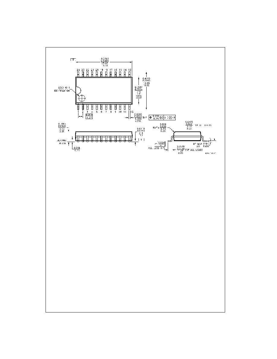
Physical Dimensions
inches (millimeters) unless otherwise noted
24-Lead Small Outline Integrated Circuit (SOIC), JEDEC MS-013, 0.300 Wide
Package Number M24B