© 1999 Fairchild Semiconductor Corporation
DS010927
www.fairchildsemi.com
May 1991
Revised November 1999
7
4
AC
TQ165
40 16-
Bit
I
n
ver
ti
ng Buf
f
er
/Li
n
e
Dri
ver
w
i
th
3-
ST
A
T
E
O
u
t
put
s
74ACTQ16540
16-Bit Inverting Buffer/Line Driver with 3-STATE Outputs
General Description
The ACTQ16540 contains sixteen inverting buffers with 3-
STATE outputs designed to be employed as a memory and
address driver, clock driver, or bus-oriented transmitter/
receiver. The device is byte controlled. Each byte has sep-
arate 3-STATE control inputs which can be shorted
together for full 16-bit operation.
The ACTQ16540 utilizes Fairchild Quiet Series
technol-
ogy to guarantee quiet output switching and improved
dynamic threshold performance. FACT Quiet Series
fea-
tures GTO
output control for superior performance.
Features
s
Utilizes Fairchild FACT Quiet Series technology
s
Guaranteed simultaneous switching noise level and
dynamic threshold performance
s
Guaranteed pin-to-pin output skew
s
Separate control logic for each byte
s
Outputs source/sink 24 mA
s
Additional specs for multiple output switching
s
Output loading specs for both 50 pF and 250 pF loads
Ordering Code:
Device also available in Tape and Reel Specify by appending suffix letter "X" to the ordering code.
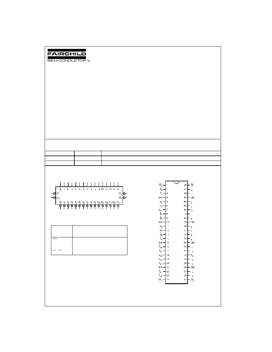
Logic Symbol
Pin Descriptions
Connection Diagram
FACT
, Quiet Series
, FACT Quiet Series
and GTO
are trademarks of Fairchild Semiconductor Corporation.
Order Number
Package Number
Package Description
74ACTQ16540SSC
MS48A
48-Lead Small Shrink Outline Package (SSOP), JEDEC MO-118, 0.300" Wide
74ACTQ16540MTD
MTD48
48-Lead Thin Shrink Small Outline Package (TSSOP), JEDEC MO-153, 6.1mm Wide
Pin
Description
Names
OE
n
Output Enable Input (Active LOW)
I
0
≠I
15
Inputs
O
0
≠O
15
Outputs
www.fairchildsemi.com
2
74ACTQ16540
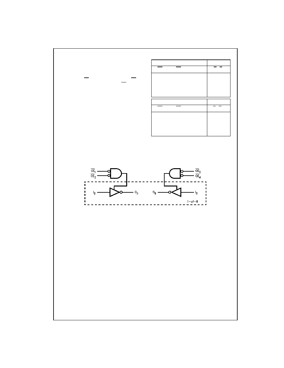
Functional Description
The ACTQ16540 contains sixteen inverting buffers with 3-
STATE standard outputs. The device is byte controlled with
each byte functioning identically, but independent of the
other. The control pins may be shorted together to obtain
full 16-bit operation. The 3-STATE outputs are controlled by
an Output Enable (OE
n
) input for each byte. When OE
n
is
LOW, the outputs are in 2-state mode. When OE
n
is HIGH,
the outputs are in the high impedance mode, but this does
not interfere with entering new data into the inputs.
Truth Tables
H
=
HIGH Voltage Level
L
=
LOW Voltage Level
X
=
Immaterial
Z
=
High Impedance
Logic Diagram
Inputs
Outputs
OE
1
OE
2
I
0
≠I
7
O
0
≠O
7
L
L
H
L
H
X
X
Z
X
H
X
Z
L
L
L
H
Inputs
Outputs
OE
3
OE
4
I
8
≠I
15
O
8
≠O
15
L
L
H
L
H
X
X
Z
X
H
X
Z
L
L
L
H
3
www.fairchildsemi.com
7
4
AC
TQ165
40
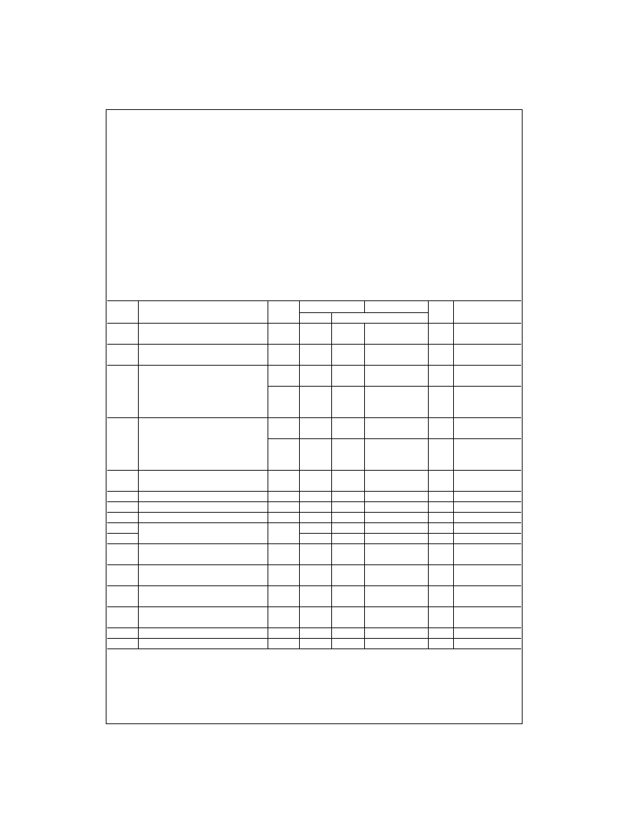
Absolute Maximum Ratings
(Note 1)
Recommended Operating
Conditions
Note 1: Absolute maximum ratings are those values beyond which damage
to the device may occur. The databook specifications should be met, with-
out exception to ensure that the system design is reliable over its power
supply, temperature, and output/input loading variables. Fairchild does not
recommend operation of FACT
circuits outside databook specifications.
DC Electrical Characteristics
Note 2: All outputs loaded; thresholds associated with output under test.
Note 3: Maximum test duration 2.0 ms; one output loaded at a time.
Note 4: Worst case package.
Note 5: Maximum number of outputs that can switch simultaneously is n. (n
-
1) outputs are switched LOW and one output held LOW.
Note 6: Maximum number of outputs that can switch simultaneously is n. (n
-
1) outputs are switched HIGH and one output held HIGH.
Note 7: Maximum number of data inputs (n) switching. (n
-
1) input switching 0V to 3V (ACTQ). Input under test switching 3V to threshold (V
ILD
).
Supply Voltage (V
CC
)
-
0.5V to
+
7.0V
DC Input Diode Current (I
IK
)
V
I
=
-
0.5V
-
20 mA
V
I
=
V
CC
+
0.5V
+
20 mA
DC Output Diode Current (I
OK
)
V
O
=
-
0.5V
-
20 mA
V
O
=
V
CC
+
0.5V
+
20 mA
DC Output Voltage (V
O
)
-
0.5V to V
CC
+
0.5V
DC Output Source/Sink Current (I
O
)
±
50 mA
DC V
CC
or Ground Current
per Output Pin
±
50 mA
Storage Temperature
-
65
∞
C to
+
150
∞
C
Supply Voltage (V
CC
)
4.5V to 5.5V
Input Voltage (V
I
)
0V to V
CC
Output Voltage (V
O
)
0V to V
CC
Operating Temperature (T
A
)
-
40
∞
C to
+
85
∞
C
Minimum Input Edge Rate (
V/
t)
125 mV/ns
V
IN
from 0.8V to 2.0V
V
CC
@ 4.5V, 5.5V
Symbol
Parameter
V
CC
T
A
=
+
25
∞
C
T
A
=
-
40
∞
C to
+
85
∞
C
Units
Conditions
(V)
Typ
Guaranteed Limits
V
IH
Minimum HIGH
4.5
1.5
2.0
2.0
V
V
OUT
=
0.1V
Input Voltage
5.5
1.5
2.0
2.0
or V
CC
-
0.1V
V
IL
Maximum LOW
4.5
1.5
0.8
0.8
V
V
OUT
=
0.1V
Input Voltage
5.5
1.5
0.8
0.8
or V
CC
-
0.1V
V
OH
Minimum HIGH
4.5
4.49
4.4
4.4
V
I
OUT
=
-
50
µ
A
Output Voltage
5.5
5.49
5.4
5.4
V
IN
=
V
IL
or V
IH
4.5
3.86
3.76
V
I
OH
=
-
24 mA
5.5
4.86
4.76
I
OH
=
-
24 mA (Note 2)
V
OL
Maximum LOW
4.5
0.001
0.1
0.1
V
I
OUT
=
50
µ
A
Output Voltage
5.5
0.001
0.1
0.1
V
IN
=
V
IL
or V
IH
4.5
0.36
0.44
V
I
OL
=
24 mA
5.5
0.36
0.44
I
OL
=
24 mA (Note 2)
I
OZ
Maximum 3-STATE
5.5
±
0.5
±
5.0
µ
A
V
I
=
V
IL
, V
IH
Leakage Current
V
O
=
V
CC
, GND
I
IN
Maximum Input Leakage Current
5.5
±
0.1
±
1.0
µ
A
V
I
=
V
CC
, GND
I
CCT
Maximum I
CC
/Input
5.5
0.6
1.5
mA
V
I
=
V
CC
-
2.1V
I
CC
Max Quiescent Supply Current
5.5
8.0
80.0
µ
A
V
IN
=
V
CC
or GND
I
OLD
Minimum Dynamic
5.5
75
mA
V
OLD
=
1.65V Max
I
OHD
Output Current (Note 3)
-
75
mA
V
OHD
=
3.85V Min
V
OLP
Quiet Output
5.0
0.5
0.8
V
Figure 1, Figure 2
Maximum Dynamic V
OL
(Note 5)(Note 6)
V
OLV
Quiet Output
5.0
-
0.5
-
1.0
V
Figure 1, Figure 2
Minimum Dynamic V
OL
(Note 5)(Note 6)
V
OHP
Maximum
5.0
V
OH
+
1.0 V
OH
+
1.5
V
Figure 1, Figure 2
Overshoot
(Note 4)(Note 6)
V
OHV
Minimum
5.0
V
OH
-
1.0 V
OH
-
1.8
V
Figure 1, Figure 2
V
CC
Droop
(Note 4)(Note 6)
V
IHD
Minimum HIGH Dynamic Input Voltage Level
5.0
1.7
2.0
V
(Note 4)(Note 7)
V
ILD
Maximum LOW Dynamic Input Voltage Level
5.0
1.2
0.8
V
(Note 4)(Note 7)
www.fairchildsemi.com
4
74ACTQ16540
AC Electrical Characteristics
Note 8: Voltage Range 5.0 is 5.0V
±
0.5V.
Extended AC Electrical Characteristics
Note 9: Voltage Range 5.0 is 5.0V
±
0.5V.
Note 10: This specification is guaranteed but not tested. The limits apply to propagation delays for all paths described switching in phase (i.e., all LOW-to-
HIGH, HIGH-to-LOW, etc.).
Note 11: This specification is guaranteed but not tested. The limits represent propagation delays with 250 pF load capacitors in place of the 50 pF load
capacitors in the standard AC load. This specification pertains to single output switching only.
Note 12: 3-STATE delays are load dominated and have been excluded from the datasheet.
Note 13: The Output Disable Time is dominated by the RC network (500
, 250 pF) on the output and has been excluded from the datasheet.
Note 14: Skew is defined as the absolute value of the difference between the actual propagation delays for any two separate outputs of the same device.
The specification applies to any outputs switching HIGH-to-LOW (t
OSHL
), LOW-to-HIGH (t
OSLH
), or any combination switching LOW-to-HIGH and/or HIGH-
to-LOW (t
OST
).
Capacitance
V
CC
T
A
=
+
25
∞
C
T
A
=
-
40
∞
C to
+
85
∞
C
Symbol
Parameter
(V)
C
L
=
50 pF
C
L
=
50 pF
Units
(Note 8)
Typ
Min
Max
Min
Max
t
PLH
Propagation Delay
5.0
2.7
4.9
7.3
2.7
7.8
ns
t
PHL
Data to Output
3.0
5.1
7.3
3.0
7.8
t
PZH
Output Enable
5.0
2.5
4.8
7.4
2.5
7.9
ns
t
PZL
Time
2.7
5.3
8.0
2.7
8.5
t
PHZ
Output Disable
5.0
2.5
5.4
8.3
2.5
8.7
ns
t
PLZ
Time
2.3
5.0
7.4
2.3
7.9
T
A
=
-
40
∞
C to
+
85
∞
C
C
L
=
50 pF
T
A
=
-
40
∞
C to
+
85
∞
C
Symbol
Parameter
V
CC
16 Outputs Switching
C
L
=
250 pF
Units
(V)
(Note 10)
(Note 11)
(Note 9)
Min
Typ
Max
Min
Max
t
PLH
Propagation Delay,
5.0
4.0
12.6
5.6
15.5
ns
t
PHL
Data to Output
4.0
10.0
5.6
13.6
t
PZH
Output Enable Time
5.0
3.2
10.8
(Note 12)
ns
t
PZL
3.4
10.8
t
PHZ
Output Disable Time
5.0
3.8
9.5
(Note 13)
ns
t
PLZ
3.1
9.2
t
OSHL
Pin to Pin Skew,
5.0
1.2
ns
(Note 14)
HL Data to Output
t
OSLH
Pin to Pin Skew,
5.0
2.5
ns
(Note 14)
LH Data to Output
t
OST
Pin to Pin Skew,
5.0
4.3
ns
(Note 14)
LH/HL Data to Output
Symbol
Parameter
Typ
Units
Conditions
C
IN
Input Pin Capacitance
4.5
pF
V
CC
=
5.0V
C
PD
Power Dissipation Capacitance
30
pF
V
CC
=
5.0V
5
www.fairchildsemi.com
7
4
AC
TQ165
40
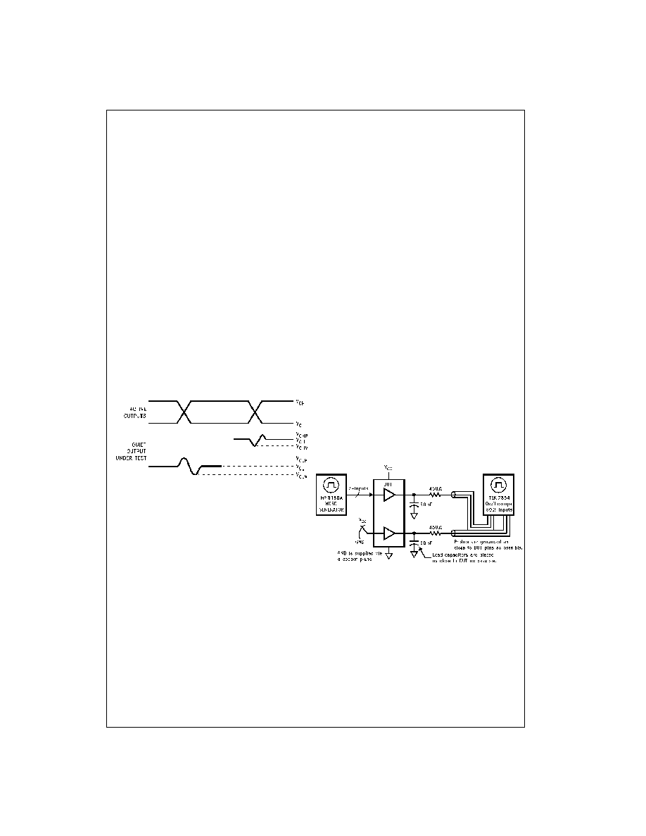
FACT Noise Characteristics
The setup of a noise characteristics measurement is critical
to the accuracy and repeatability of the tests. The following
is a brief description of the setup used to measure the
noise characteristics of FACT.
Equipment:
Hewlett Packard Model 8180A Word Generator
PC-163A Test Fixture
Tektronics Model 7854 Oscilloscope
Procedure:
1. Verify Test Fixture Loading: Standard Load 50 pF,
500
.
2. Deskew the HFS generator so that no two channels
have greater than 150 ps skew between them. This
requires that the oscilloscope be deskewed first. It is
important to deskew the HFS generator channels
before testing. This will ensure that the outputs switch
simultaneously.
3. Terminate all inputs and outputs to ensure proper load-
ing of the outputs and that the input levels are at the
correct voltage.
4. Set the HFS generator to toggle all but one output at a
frequency of 1 MHz. Greater frequencies will increase
DUT heating and effect the results of the measure-
ment.
5. Set the word generator input levels at 0V LOW and 3V
HIGH for ACT devices and 0V LOW and 5V HIGH for
AC devices. Verify levels with an oscilloscope.
V
OHV
and V
OLP
are measured with respect to ground reference.
Input pulses have the following characteristics: f
=
1 MHz, t
r
=
3 ns,
t
f
=
3 ns, skew
<
150 ps.
FIGURE 1. Quiet Output Noise Voltage Waveforms
V
OLP
/V
OLV
and V
OHP
/V
OHV
:
∑ Determine the quiet output pin that demonstrates the
greatest noise levels. The worst case pin will usually be
the furthest from the ground pin. Monitor the output volt-
ages using a 50
coaxial cable plugged into a standard
SMB type connector on the test fixture. Do not use an
active FET probe.
∑ Measure V
OLP
and V
OLV
on the quiet output during the
worst case transition for active and enable. Measure
V
OHP
and V
OHV
on the quiet output during the worst
case transition for active and enable.
∑ Verify that the GND reference recorded on the oscillo-
scope has not drifted to ensure the accuracy and repeat-
ability of the measurements.
V
ILD
and V
IHD
:
∑ Monitor one of the switching outputs using a 50
coaxial
cable plugged into a standard SMB type connector on
the test fixture. Do not use an active FET probe.
∑ First increase the input LOW voltage level, V
IL
, until the
output begins to oscillate or steps out a min of 2 ns.
Oscillation is defined as noise on the output LOW level
that exceeds V
IL
limits, or on output HIGH levels that
exceed V
IH
limits. The input LOW voltage level at which
oscillation occurs is defined as V
ILD
.
∑ Next decrease the input HIGH voltage level, V
IH
, until
the output begins to oscillate or steps out a min of 2 ns.
Oscillation is defined as noise on the output LOW level
that exceeds V
IL
limits, or on output HIGH levels that
exceed V
IH
limits. The input HIGH voltage level at which
oscillation occurs is defined as V
IHD
.
∑ Verify that the GND reference recorded on the oscillo-
scope has not drifted to ensure the accuracy and repeat-
ability of the measurements.
FIGURE 2. Simultaneous Switching Test Circuit
www.fairchildsemi.com
6
74ACTQ16540
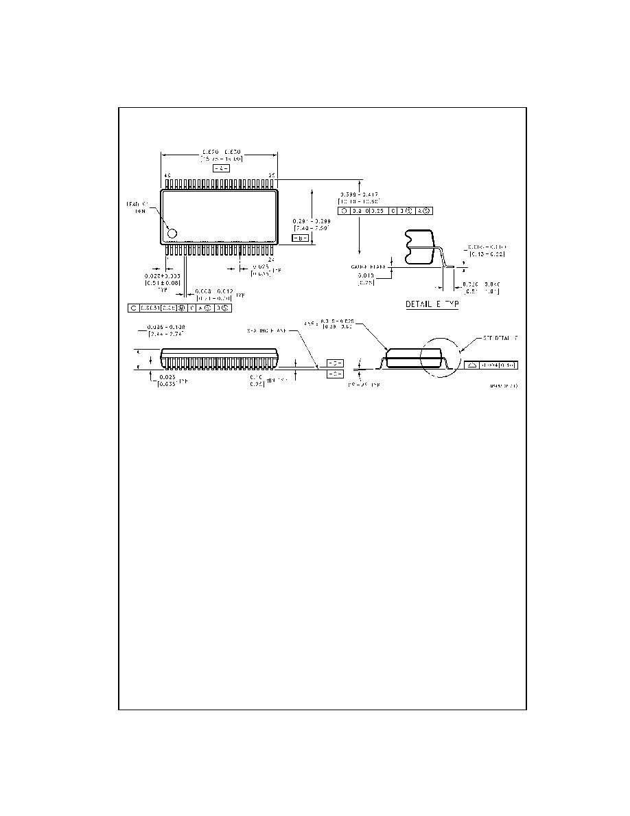
Physical Dimensions
inches (millimeters) unless otherwise noted
48-Lead Small Shrink Outline Package (SSOP), JEDEC MO-118, 0.300" Wide
Package Number MS48A
7
www.fairchildsemi.com
7
4
AC
TQ165
40 16-
Bit
I
n
ver
ti
ng Buf
f
er
/Li
n
e
Dri
ver
w
i
th
3-
ST
A
T
E
O
u
t
put
s
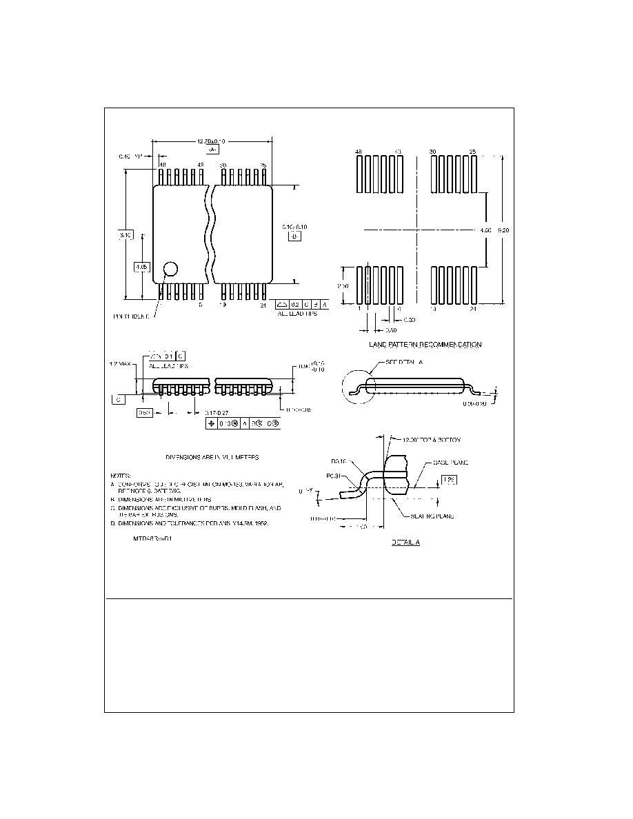
Physical Dimensions
inches (millimeters) unless otherwise noted (Continued)
48-Lead Thin Shrink Small Outline Package (TSSOP), JEDEC MO-153, 6.1mm Wide
Package Number MTD48
Fairchild does not assume any responsibility for use of any circuitry described, no circuit patent licenses are implied and
Fairchild reserves the right at any time without notice to change said circuitry and specifications.
LIFE SUPPORT POLICY
FAIRCHILD'S PRODUCTS ARE NOT AUTHORIZED FOR USE AS CRITICAL COMPONENTS IN LIFE SUPPORT
DEVICES OR SYSTEMS WITHOUT THE EXPRESS WRITTEN APPROVAL OF THE PRESIDENT OF FAIRCHILD
SEMICONDUCTOR CORPORATION. As used herein:
1. Life support devices or systems are devices or systems
which, (a) are intended for surgical implant into the
body, or (b) support or sustain life, and (c) whose failure
to perform when properly used in accordance with
instructions for use provided in the labeling, can be rea-
sonably expected to result in a significant injury to the
user.
2. A critical component in any component of a life support
device or system whose failure to perform can be rea-
sonably expected to cause the failure of the life support
device or system, or to affect its safety or effectiveness.
www.fairchildsemi.com