74ACTQ16543 16-Bit Registered Transceiver with 3-STATE Outputs
December 1991
Revised December 1998
7
4
A
C
TQ16543 16-
Bit
Regi
ster
ed T
r
ans
ceiver
wi
th 3-ST
A
T
E
Out
puts
© 1999 Fairchild Semiconductor Corporation
DS010967.prf
www.fairchildsemi.com
74ACTQ16543
16-Bit Registered Transceiver with 3-STATE Outputs
General Description
The ACTQ16543 contains sixteen non-inverting transceiv-
ers containing two sets of D-type registers for temporary
storage of data flowing in either direction. Each byte has
separate control inputs which can be shorted together for
full 16-bit operation. Separate Latch Enable and Output
Enable inputs are provided for each register to permit inde-
pendent input and output control in either direction of data
flow.
The ACTQ16543 utilizes Fairchild Quiet Series
TM
technol-
ogy to guarantee quiet output switching and improved
dynamic threshold performance. FACT Quiet Series
TM
fea-
tures GTO
TM
output control and undershoot corrector for
superior performance.
Features
s
Utilizes Fairchild FACT Quiet Series technology
s
Guaranteed simultaneous switching noise level and
dynamic threshold performance
s
Guaranteed pin-to-pin output skew
s
Independent registers for A and B buses
s
Separate controls for data flow in each direction
s
Back-to-back registers for storage
Multiplexed real-time and stored data transfers
s
Separate control logic for each byte
s
16-bit version of the ACTQ543
s
Outputs source/sink 24 mA
s
Additional specs for Multiple Output Switching
s
Output loading specs for both 50 pF and 250pF loads
Ordering Code:
Device also available in Tape and Reel. Specify by appending suffix letter "X" to the ordering code.
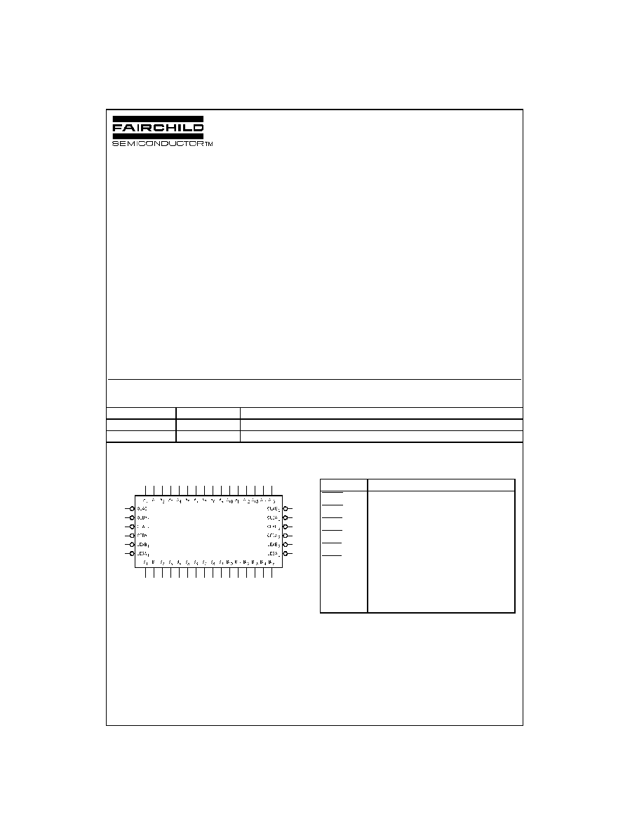
Logic Symbol
Pin Descriptions
FACT
TM
, Quiet Series
TM
, FACT Quiet Series
TM
and GTO
TM
are trademarks of Fairchild Semiconductor Corporation.
Order Number
Package Number
Package Description
74ACTQ16543SSC
MS56A
56-Lead Shrink Small Outline Package (SSOP), JEDEC MO-118, 0.300" Wide
74ACTQ16543MTD
MTD56
56-Lead Thin Shrink Small Outline Package (TSSOP), JEDEC MO-153, 6.1mm Wide
Pin Names
Descriptions
OEAB
n
A-to-B Output Enable Input (Active LOW)
OEBA
n
B-to-A Output Enable Input (Active LOW)
CEAB
n
A-to-B Enable Input (Active LOW)
CEBA
n
B-to-A Enable Input (Active LOW)
LEAB
n
A-to-B Latch Enable Input (Active LOW)
LEBA
n
B-to-A Latch Enable Input (Active LOW)
A
0
A
15
A-to-B Data Inputs or
B-to-A 3-STATE Outputs
B
0
B
15
B-to-A Data Inputs or
A-to-B 3-STATE Outputs
www.fairchildsemi.com
2
74A
CTQ16543
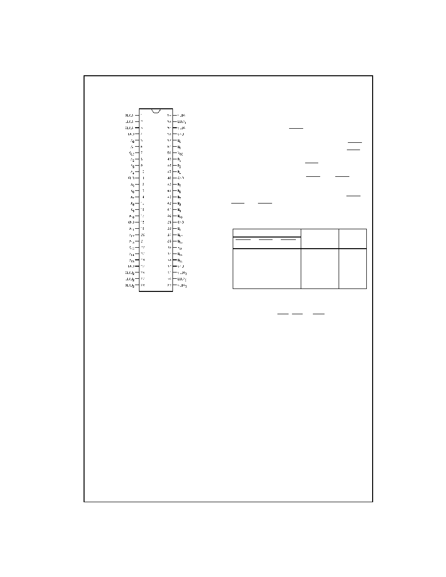
Connection Diagram
Pin Assignment for SSOP and TSSOP
Functional Description
The ACTQ16543 contains sixteen non-inverting transceiv-
ers with 3-STATE outputs. The device is byte controlled
with each byte functioning identically, but independent of
the other. The control pins may be shorted together to
obtain full 16-bit operation. The following description
applies to each byte. For data flow from A to B, for exam-
ple, the A-to-B Enable (CEAB
n
) input must be LOW in
order to enter data from A
0
A
15
or take data from B
0
B
15
,
as indicated in the Data I/O Control Table. With CEAB
n
LOW, a LOW signal on the A-to-B Latch Enable (LEAB
n
)
input makes the A-to-B latches transparent; a subsequent
LOW-to-HIGH transition of the LEAB
n
signal puts the A
latches in the storage mode and their outputs no longer
change with the A inputs. With CEAB
n
and OEAB
n
both
LOW, the 3-STATE B output buffers are active and reflect
the data present at the output of the A latches. Control of
data flow from B to A is similar, but using the CEBA
n
,
LEBA
n
and OEBA
n
inputs.
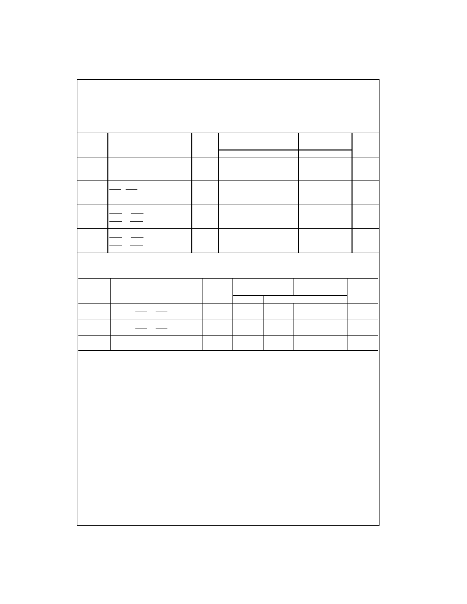
Data I/O Control Table
H
=
HIGH Voltage Level
L
=
LOW Voltage Level
X
=
Immaterial
A-to-B data flow shown; B-to-A flow control
is the same, except using CEBA
n
, LEBA
n
and OEBA
n
Inputs
Latch Status
(Byte n)
Output
Buffers
(Byte n)
CEAB
n
LEAB
n
OEAB
n
H
X
X
Latched
High Z
X
H
X
Latched
--
L
L
X
Transparent
--
X
X
H
--
High Z
L
X
L
--
Driving
3
www.fairchildsemi.com
7
4
A
C
TQ16543
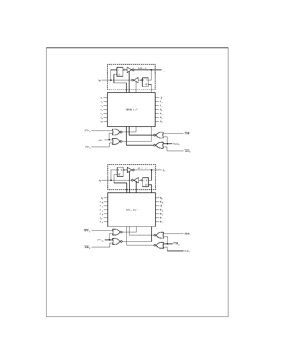
Logic Diagrams
Byte 1 (0:7)
Please note that this diagram is provided only for the understanding of logic operations and should not be used to estimate propagation delays.
Byte 2 (8:15)
Please note that this diagram is provided only for the understanding of logic operations and should not be used to estimate propagation delays.
www.fairchildsemi.com
4
74A
CTQ16543
Absolute Maximum Ratings
(Note 1)
Recommended Operating
Conditions
Note 1: Absolute maximum ratings are those values beyond which damage
to the device may occur. The databook specifications should be met, with-
out exception, to ensure that the system design is reliable over its power
supply, temperature, and output/input loading variables. Fairchild does not
recommend operation of FACT
TM
circuits outside databook specifications.
DC Electrical Characteristics
Note 2: All outputs loaded; thresholds associated with output under test.
Note 3: Maximum test duration 2.0 ms; one output loaded at a time.
Note 4: Worst case package.
Supply Voltage (V
CC
)
-
0.5V to
+
7.0V
DC Input Diode Current (I
IK
)
V
I
=
-
0.5V
-
20 mA
V
I
=
V
CC
+
0.5V
+
20 mA
DC Output Diode Current (I
OK
)
V
O
=
-
0.5V
-
20 mA
V
O
=
V
CC
+
0.5V
+
20 mA
DC Output Voltage (V
O
)
-
0.5V to V
CC
+
0.5V
DC Output Source/Sink Current (I
O
)
±
50 mA
DC V
CC
or Ground Current
per Output Pin
±
50 mA
Storage Temperature
-
65
°
C to
+
150
°
C
Supply Voltage (V
CC
)
4.5V to 5.5V
Input Voltage (V
I
)
0V to V
CC
Output Voltage (V
O
)
0V to V
CC
Operating Temperature (T
A
)
-
40
°
C to
+
85
°
C
Minimum Input Edge Rate (
V/
t)
125 mV/ns
V
IN
from 0.8V to 2.0V
V
CC
@ 4.5V, 5.5V
Symbol
Parameter
V
CC
T
A
=
+
25
°
C
T
A
=
-
40
°
C to
+
85
°
C
Units
Conditions
(V)
Typ
Guaranteed Limits
V
IH
Minimum HIGH
4.5
1.5
2.0
2.0
V
V
OUT
=
0.1V
Input Voltage
5.5
1.5
2.0
2.0
or V
CC
-
0.1V
V
IL
Maximum LOW
4.5
1.5
0.8
0.8
V
V
OUT
=
0.1V
Input Voltage
5.5
1.5
0.8
0.8
or V
CC
-
0.1V
V
OH
Minimum HIGH
4.5
4.49
4.4
4.4
V
I
OUT
=
-
50
µ
A
Output Voltage
5.5
5.49
5.4
5.4
V
IN
=
V
IL
or V
IH
4.5
3.86
3.76
V
I
OH
=
-
24 mA
5.5
4.86
4.76
I
OH
=
-
24 mA (Note 2)
V
OL
Maximum LOW
4.5
0.001
0.1
0.1
V
I
OUT
=
50
µ
A
Output Voltage
5.5
0.001
0.1
0.1
V
IN
=
V
IL
or V
IH
4.5
0.36
0.44
V
I
OL
= 24 mA
5.5
0.36
0.44
I
OL
= 24 mA (Note 2)
I
OZT
Maximum I/O
5.5
±
0.5
±
5.0
µ
A
V
I
=
V
IL
, V
IH
Leakage Current
V
O
=
V
CC
, GND
I
IN
Maximum Input
5.5
±
0.1
±
1.0
µ
A
V
I
=
V
CC
,
Leakage Current
GND
I
CCT
Maximum I
CC
/Input
5.5
0.6
1.5
mA
V
I
=
V
CC
-
2.1V
I
CC
Max Quiescent
5.5
8.0
80.0
µ
A
V
IN
=
V
CC
Supply Current
or GND
I
OLD
Minimum Dynamic
5.5
75
mA
V
OLD
=
1.65V Max
I
OHD
Output Current (Note 3)
-
75
mA
V
OHD
=
3.85V Min
V
OLP
Quiet Output
5.0
0.5
0.8
V
Figure 1, Figure 2
Maximum Dynamic V
OL
(Note 5)(Note 6)
V
OLV
Quiet Output
5.0
-
0.5
-
0.8
V
Figure 1, Figure 2
Minimum Dynamic V
OL
(Note 5)(Note 6)
V
OHP
Maximum
5.0
V
OH
+
1.0
V
OH
+
1.5
V
Figure 1, Figure 2
Overshoot
(Note 4)(Note 6)
V
OHV
Minimum
5.0
V
OH
-
1.0
V
OH
-
1.8
V
Figure 1, Figure 2
V
CC
Droop
(Note 4)(Note 6)
V
IHD
Minimum HIGH Dynamic
5.0
1.7
2.0
V
(Note 4)(Note 7)
Input Voltage Level
V
ILD
Maximum LOW Dynamic
5.0
1.2
0.8
V
(Note 4)(Note 7)
Input Voltage Level
5
www.fairchildsemi.com
7
4
A
C
TQ16543
DC Electrical Characteristics
(Continued)
Note 5: Maximum number of outputs that can switch simultaneously is n. (n
-
1) outputs are switched LOW and one output held LOW.
Note 6: Maximum number of outputs that can switch simultaneously is n. (n
-
1) outputs are switched HIGH and one output held HIGH.
Note 7: Maximum number of data inputs (n) switching. (n
-
1) inputs switching 0V to 3V Input under test switching 3V to threshold (V
ILD
).
AC Electrical Characteristics
Note 8: Voltage Range 5.0 is 5.0V
±
0.5V.
AC Operating Requirements
Note 9: Voltage Range 5.0 is 5.0V
±
0.5V
V
CC
T
A
=
+
25
°
C
T
A
=
-
40
°
C to
+
85
°
C
Symbol
Parameter
(V)
C
L
=
50 pF
C
L
=
50 pF
Units
(Note 8)
Min
Typ
Max
Min
Max
t
PLH
Propagation Delay
3.8
5.9
8.3
3.0
9.0
t
PHL
Transparent Mode
5.0
3.5
5.5
7.9
2.6
8.5
ns
A
n
to B
n
or B
n
to A
n
t
PLH
Propagation Delay
4.7
6.9
9.8
3.4
10.8
t
PHL
LEBA
n
, LEAB
n
5.0
3.9
6.3
9.0
3.1
9.8
ns
to A
n
, B
n
t
PZH
Output Enable Time
4.2
6.3
9.2
3.0
9.9
t
PZL
OEBA
n
or OEAB
n
to A
n
or B
n
5.0
4.9
7.3
10.3
3.6
10.3
ns
CEBA
n
or CEAB
n
to A
n
or B
n
t
PHZ
Output Disable Time
2.8
5.2
8.0
2.1
8.3
t
PLZ
OEBA
n
or OEAB
n
to A
n
or B
n
5.0
2.6
5.0
7.6
2.0
8.1
ns
CEBA
n
or CEAB
n
to A
n
or B
n
V
CC
T
A
=
+
25
°
C
T
A
=
-
40
°
C to
+
85
°
C
Symbol
Parameter
(V)
C
L
=
50 pF
C
L
=
50 pF
Units
(Note 9)
Typ
Guaranteed Minimum
t
S
Setup Time, HIGH or LOW
5.0
3.0
3.0
ns
A
n
or B
n
to LEBA
n
or LEAB
n
t
H
Hold Time, HIGH or LOW
5.0
1.5
1.5
ns
A
n
or B
n
to LEBA
n
or LEAB
n
t
W
Latch Enable, B to A
5.0
4.0
4.0
ns
Pulse Width, LOW
www.fairchildsemi.com
6
74A
CTQ16543
Extended AC Electrical Characteristics
Note 10: This specification is guaranteed but not tested. The limits apply to propagation delays for all paths described switching in phase (i.e., all low-to-high,
high-to-low, etc.).
Note 11: This specification is guaranteed but not tested. The limits represent propagation delays with 250 pF load capacitors in place of the 50 pF load
capacitors in the standard AC load. This specification pertains to single output switching only.
Note 12: 3-STATE delays are load dominated and have been excluded from the datasheet.
Note 13: The Output Disable Time is dominated by the RC network (500
, 250 pF) on the output and has been excluded from the datasheet.
Note 14: Skew is defined as the absolute value of the difference between the actual propagation delays for any two separate outputs of the same device.
The specification applies to any outputs switching HIGH to LOW (t
OSHL
), LOW to HIGH (t
OSLH
), or any combination switching LOW to HIGH and/or HIGH to
LOW (t
OST
).
Capacitance
T
A
=
-
40 to
+
85
°
C
V
CC
=
Com
T
A
=
-
40 to
+
85
°
C
Symbol
Parameter
C
L
=
50 pF
V
CC
=
Com
Units
16 Outputs Switching
C
L
=
250 pF
(Note 10)
(Note 11)
Min
Typ
Max
Min
Max
t
PLH
Propagation Delay
4.5
11.1
5.8
14.3
t
PHL
Transparent Mode
3.7
9.6
5.1
13.4
ns
A
n
to B
n
or B
n
to A
n
t
PLH
Propagation Delay
4.3
11.3
6.2
16.3
ns
t
PHL
LEBA
n
, LEAB
n
to A
n
, B
n
3.7
9.7
5.8
14.9
t
PZH
Output Enable Time
4.0
10.7
t
PZL
OEBA
n
or OEAB
n
to A
n
or B
n
4.3
11.3
(Note 12)
ns
CEBA
n
or CEAB
n
to A
n
or B
n
t
PHZ
Output Disable Time
3.0
8.0
t
PLZ
OEBA
n
or OEAB
n
to A
n
or B
n
2.8
7.6
(Note 13)
ns
CEBA
n
or CEAB
n
to A
n
or B
n
t
OSHL
Pin to Pin Skew
1.1
ns
(Note 14)
HL Data to Output
t
OSLH
Pin to Pin Skew
1.4
ns
(Note 14)
LH Data to Output
t
OSHL
Pin to Pin Skew
2.6
ns
(Note 14)
Latch to Output
t
OSLH
Pin to Pin Skew
1.0
ns
(Note 14)
Latch to Output
t
OST
Pin to Pin Skew
1.0
ns
(Note 14)
Data to Output
t
OST
Pin to Pin Skew
2.2
ns
(Note 14)
Latch to Output
Symbol
Parameter
Typ
Units
Conditions
C
IN
Input Capacitance
4.5
pF
V
CC
=
5.0V
C
PD
Power Dissipation.Capacitance
95.0
pF
V
CC
=
5.0V
7
www.fairchildsemi.com
7
4
A
C
TQ16543
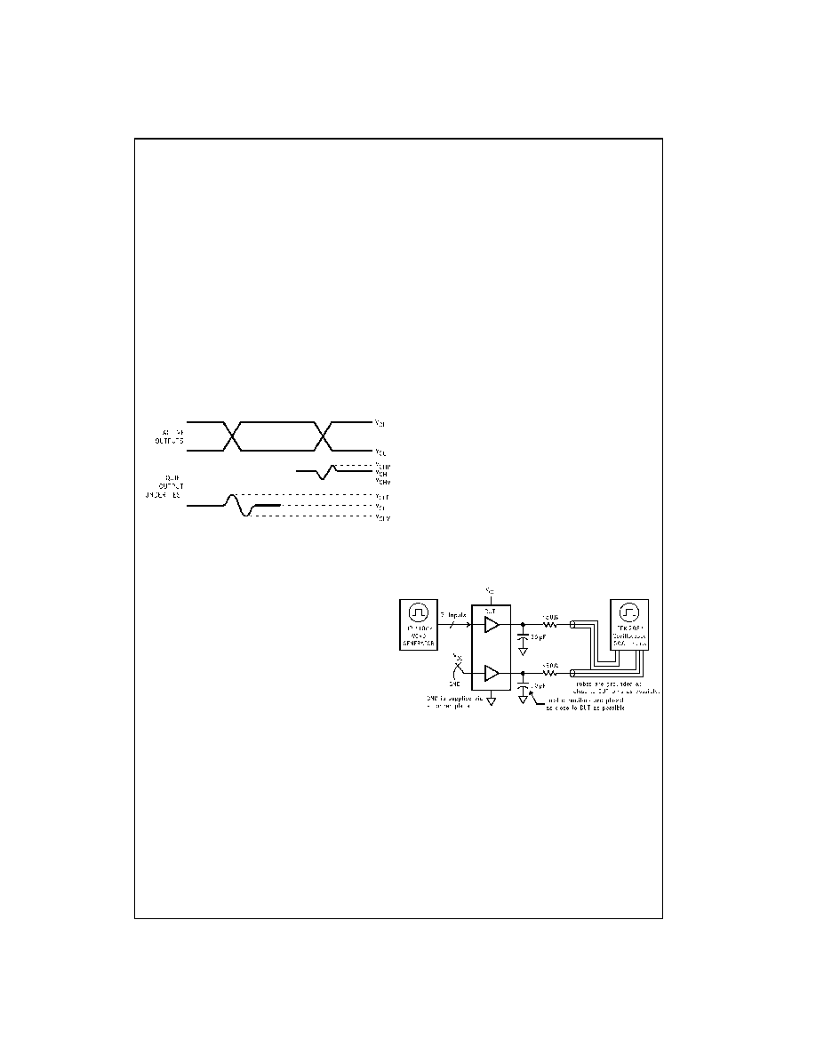
FACT Noise Characteristics
The setup of a noise characteristics measurement is critical
to the accuracy and repeatability of the tests. The following
is a brief description of the setup used to measure the
noise characteristics of FACT.
Equipment:
Hewlett Packard Model 8180A Word Generator
PC-163A Test Fixture
Tektronics Model 7854 Oscilloscope
Procedure:
1. Verify Test Fixture Loading: Standard Load 50 pF,
500
.
2. Deskew the HFS generator so that no two channels
have greater than 150 ps skew between them. This
requires that the oscilloscope be deskewed first. It is
important to deskew the HFS generator channels
before testing. This will ensure that the outputs switch
simultaneously.
3. Terminate all inputs and outputs to ensure proper load-
ing of the outputs and that the input levels are at the
correct voltage.
4.
V
OHV
and V
OLP
are measured with respect to ground reference.
Input pulses have the following characteristics: f
=
1 MHz, t
r
=
3 ns, t
f
=
3 ns, skew
<
150 ps.
FIGURE 1. Quiet Output Noise Voltage Waveforms
5. Set the HFS generator to toggle all but one output at a
frequency of 1 MHz. Greater frequencies will increase
DUT heating and effect the results of the measure-
ment.
6. Set the HFS generator input levels at 0V LOW and 3V
HIGH for ACT devices and 0V LOW and 5V HIGH for
AC devices. Verify levels with an oscilloscope.
V
OLP
/V
OLV
and V
OHP
/V
OHV
:
· Determine the quiet output pin that demonstrates the
greatest noise levels. The worst case pin will usually be
the furthest from the ground pin. Monitor the output volt-
ages using a 50
coaxial cable plugged into a standard
SMB type connector on the test fixture. Do not use an
active FET probe.
· Measure V
OLP
and V
OLV
on the quiet output during the
worst case transition for active and enable. Measure
V
OHP
and V
OHV
on the quiet output during the worst
case for active and enable transition.
· Verify that the GND reference recorded on the oscillo-
scope has not drifted to ensure the accuracy and repeat-
ability of the measurements.
V
ILD
and V
IHD
:
· Monitor one of the switching outputs using a 50
coaxial
cable plugged into a standard SMB type connector on
the test fixture. Do not use an active FET probe.
· First increase the input LOW voltage level, V
IL
, until the
output begins to oscillate or steps out a min of 2 ns.
Oscillation is defined as noise on the output LOW level
that exceeds V
IL
limits, or on output HIGH levels that
exceed V
IH
limits. The input LOW voltage level at which
oscillation occurs is defined as V
ILD
.
· Next decrease the input HIGH voltage level, V
IH
, until
the output begins to oscillate or steps out a min of 2 ns.
Oscillation is defined as noise on the output LOW level
that exceeds V
IL
limits, or on output HIGH levels that
exceed V
IH
limits. The input HIGH voltage level at which
oscillation occurs is defined as V
IHD
.
· Verify that the GND reference recorded on the oscillo-
scope has not drifted to ensure the accuracy and repeat-
ability on the measurements.
FIGURE 2. Simultaneous Switching Test Circuit
www.fairchildsemi.com
8
74A
CTQ16543
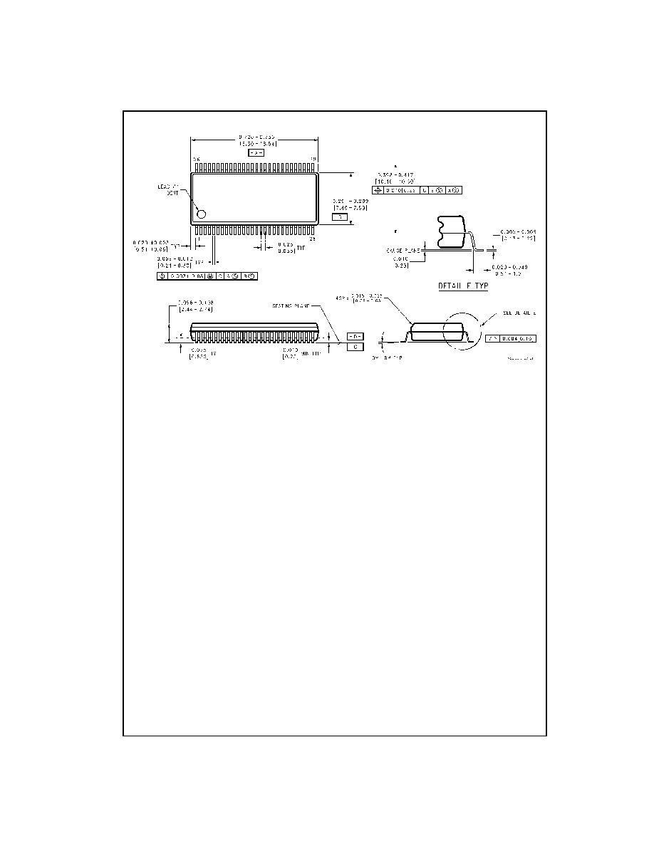
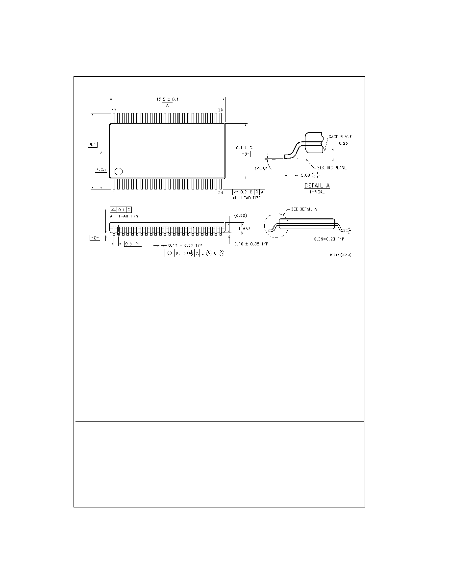
Physical Dimensions
inches (millimeters) unless otherwise noted
56-Lead Thin Shrink Small Outline Package (SSOP), JEDEC MO-153, 6.1mm Wide
Package Number MS56A
Fairchild does not assume any responsibility for use of any circuitry described, no circuit patent licenses are implied and Fairchild reserves the right at any time without notice to change said circuitry and specifications.
7
4
A
C
TQ16543 16-
Bit
Regi
ster
ed T
r
ans
ceiver
wi
th 3-ST
A
T
E
Out
puts
LIFE SUPPORT POLICY
FAIRCHILD'S PRODUCTS ARE NOT AUTHORIZED FOR USE AS CRITICAL COMPONENTS IN LIFE SUPPORT
DEVICES OR SYSTEMS WITHOUT THE EXPRESS WRITTEN APPROVAL OF THE PRESIDENT OF FAIRCHILD
SEMICONDUCTOR CORPORATION. As used herein:
1. Life support devices or systems are devices or systems
which, (a) are intended for surgical implant into the
body, or (b) support or sustain life, and (c) whose failure
to perform when properly used in accordance with
instructions for use provided in the labeling, can be rea-
sonably expected to result in a significant injury to the
user.
2. A critical component in any component of a life support
device or system whose failure to perform can be rea-
sonably expected to cause the failure of the life support
device or system, or to affect its safety or effectiveness.
www.fairchildsemi.com
Physical Dimensions
inches (millimeters) unless otherwise noted (Continued)
56-Lead Thin Shrink Small Outline Package (TSSOP), JEDEC MO-153, 6.1mm Wide
Package Number MTD56