© 1999 Fairchild Semiconductor Corporation
DS010238
www.fairchildsemi.com
July 1989
Revised November 1999
7
4
AC
Q374 ∑ 74AC
T
Q
3
7
4
Qui
e
t Seri
es
Oct
a
l D-T
y
pe Fl
ip-
F
lop wit
h
3
-
ST
A
T
E
Output
s
74ACQ374 ∑ 74ACTQ374
Quiet Series
Octal D-Type Flip-Flop
with 3-STATE Outputs
General Description
The ACQ/ACTQ374 is a high-speed, low-power octal D-
type flip-flop featuring separate D-type inputs for each flip-
flop and 3-STATE outputs for bus-oriented applications. A
buffered Clock (CP) and Output Enable (OE) are common
to all flip-flops.
The ACQ/ACTQ374 utilizes FACT Quiet Series
technol-
ogy to guarantee quiet output switching and improve
dynamic threshold performance. FACT Quiet Series fea-
tures GTO
output control and undershoot corrector in
addition to a split ground bus for superior performance.
Features
s
I
CC
and I
OZ
reduced by 50%
s
Guaranteed simultaneous switching noise level and
dynamic threshold performance
s
Guaranteed pin-to-pin skew AC performance
s
Improved latch-up immunity
s
Buffered positive edge-triggered clock
s
3-STATE outputs drive bus lines or buffer memory
address registers
s
Outputs source/sink 24 mA
s
Faster prop delays than the standard AC/ACT374
Ordering Code:
Device also available in Tape and Reel. Specify by appending suffix letter "X" to the ordering code.
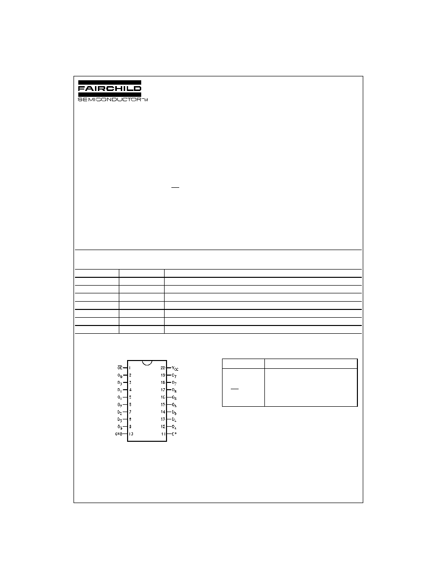
Connection Diagram
Pin Descriptions
FACT
, Quiet Series
, FACT Quiet Series
, and GTO
are trademarks of Fairchild Semiconductor Corporation.
Order Number
Package Number
Package Description
74ACQ374SC
M20B
20-Lead Small Outline Integrated Circuit (SOIC), JEDEC MS-013, 0.300" Wide Body
74ACQ374SJ
M20D
20-Lead Small Outline Package (SOP), EIAJ TYPE II, 5.3mm Wide
74ACQ374PC
N20A
20-Lead Plastic Dual-In-Line Package (PDIP), JEDEC MS-001, 0.300" Wide
74ACTQ374SC
M20B
20-Lead Small Outline Integrated Circuit (SOIC), JEDEC MS-013, 0.300" Wide Body
74ACTQ374SJ
M20D
20-Lead Small Outline Package (SOP), EIAJ TYPE II, 5.3mm Wide
74ACTQ374QSC
MQA20
20-Lead Quarter Size Outline Package (QSOP), JEDEC MO-137, 0.150" Wide
74ACTQ374PC
N20A
20-Lead Plastic Dual-In-Line Package (PDIP), JEDEC MS-001, 0.300" Wide
Pin Names
Description
D
0
≠D
7
Data Inputs
CP
Clock Pulse Input
OE
3-STATE Output Enable Input
O
0
≠O
7
3-STATE Outputs
www.fairchildsemi.com
2
74
A
C
Q374
∑
7
4
AC
T
Q
374
Logic Symbols
IEEE/IEC
Functional Description
The ACQ/ACTQ374 consists of eight edge-triggered flip-
flops with individual D-type inputs and 3-STATE true out-
puts. The buffered clock and buffered Output Enable are
common to all flip-flops. The eight flip-flops will store the
state of their individual D-type inputs that meet the setup
and hold time requirements on the LOW-to-HIGH Clock
(CP) transition. With the Output Enable (OE) LOW, the
contents of the eight flip-flops are available at the outputs.
When the OE is HIGH, the outputs go to the high imped-
ance state. Operation of the OE input does not affect the
state of the flip-flops.
Truth Table
H
=
HIGH Voltage Level
L
=
LOW Voltage Level
X
=
Immaterial
Z
=
High Impedance
=
LOW-to-HIGH Transition
Logic Diagram
Please note that this diagram is provided only for the understanding of logic operations and should not be used to estimate propagation delays.
Inputs
Outputs
D
n
CP
OE
O
n
H
L
H
L
L
L
X
X
H
Z
3
www.fairchildsemi.com
7
4
AC
Q374
∑
74AC
T
Q
3
7
4
Absolute Maximum Ratings
(Note 1)
Recommended Operating
Conditions
Note 1: Absolute maximum ratings are those values beyond which damage
to the device may occur. The databook specifications should be met, with-
out exception, to ensure that the system design is reliable over its power
supply, temperature, and output/input loading variables. Fairchild does not
recommend operation of FACT
circuits outside databook specifications.
DC Electrical Characteristics for ACQ
Supply Voltage (V
CC
)
-
0.5V to
+
7.0V
DC Input Diode Current (I
IK
)
V
I
=
-
0.5V
-
20 mA
V
I
=
V
CC
+
0.5V
+
20 mA
DC Input Voltage (V
I
)
-
0.5V to V
CC
+
0.5V
DC Output Diode Current (I
OK
)
V
O
=
-
0.5V
-
20 mA
V
O
=
V
CC
+
0.5V
+
20 mA
DC Output Voltage (V
O
)
-
0.5V to V
CC
+
0.5V
DC Output Source
or Sink Current (I
O
)
±
50 mA
DC V
CC
or Ground Current
per Output Pin (I
CC
or I
GND
)
±
50 mA
Storage Temperature (T
STG
)
-
65
∞
C to
+
150
∞
C
DC Latch-Up Source or Sink Current
±
300 mA
Junction Temperature (T
J
)
PDIP
140
∞
C
Supply Voltage (V
CC
)
ACQ
2.0V to 6.0V
ACTQ
4.5V to 5.5V
Input Voltage (V
I
)
0V to V
CC
Output Voltage (V
O
)
0V to V
CC
Operating Temperature (T
A
)
-
40
∞
C to
+
85
∞
C
Minimum Input Edge Rate
V/
t
ACQ Devices
V
IN
from 30% to 70% of V
CC
V
CC
@ 3.0V, 4.5V, 5.5V
125 mV/ns
Minimum Input Edge Rate
V/
t
ACTQ devices
V
IN
from 0.8V to 2.0V
V
CC
@ 4.5V, 5.5V
125 mV/ns
Symbol
Parameter
V
CC
T
A
=
+
25
∞
C
T
A
=
-
40
∞
C to
+
85
∞
C
Units
Conditions
(V)
Typ
Guaranteed Limits
V
IH
Minimum HIGH Level
3.0
1.5
2.1
2.1
V
OUT
=
0.1V
Input Voltage
4.5
2.25
3.15
3.15
V
or V
CC
-
0.1V
5.5
2.75
3.85
3.85
V
IL
Maximum LOW Level
3.0
1.5
0.9
0.9
V
OUT
=
0.1V
Input Voltage
4.5
2.25
1.35
1.35
V
or V
CC
-
0.1V
5.5
2.75
1.65
1.65
V
OH
Minimum HIGH Level
3.0
2.99
2.9
2.9
Output Voltage
4.5
4.49
4.4
4.4
V
I
OUT
=
-
50
µ
A
5.5
5.49
5.4
5.4
V
IN
=
V
IL
or V
IH
3.0
2.56
2.46
I
OH
=
-
12 mA
4.5
3.86
3.76
V
I
OH
=
-
24 mA
5.5
4.86
4.76
I
OH
=
-
24 mA (Note 2)
V
OL
Maximum LOW Level
3.0
0.002
0.1
0.1
Output Voltage
4.5
0.001
0.1
0.1
V
I
OUT
=
50
µ
A
5.5
0.001
0.1
0.1
3.0
0.36
0.44
I
OL
=
12 mA
4.5
0.36
0.44
V
I
OL
=
24 mA
5.5
0.36
0.44
I
OL
=
24 mA (Note 2)
I
IN
(Note 4)
Maximum Input Leakage Current
5.5
±
0.1
±
1.0
µ
A
V
I
=
V
CC
, GND
I
OLD
Minimum Dynamic
5.5
75
mA
V
OLD
=
1.65V Max
I
OHD
Output Current (Note 3)
5.5
-
75
mA
V
OHD
=
3.85V Min
I
CC
(Note 4) Maximum Quiescent Supply Current
5.5
4.0
40.0
µ
A
V
IN
=
V
CC
or GND
I
OZ
Maximum 3-STATE
V
I
(OE)
=
V
IL
, V
IH
Leakage Current
5.5
±
0.25
±
2.5
µ
A
V
I
=
V
CC
, GND
V
O
=
V
CC
, GND
V
OLP
Quiet Output
5.0
1.1
1.5
V
Figure 1, Figure 2
Maximum Dynamic V
OL
(Note 5)(Note 6)
www.fairchildsemi.com
4
74
A
C
Q374
∑
7
4
AC
T
Q
374
DC Electrical Characteristics for ACQ
(Continued)
Note 2: All outputs loaded; thresholds on input associated with output under test.
Note 3: Maximum test duration 2.0 ms, one output loaded at a time.
Note 4: I
IN
and I
CC
@ 3.0V are guaranteed to be less than or equal to the respective limit @ 5.5V V
CC
.
Note 5: DIP Package.
Note 6: Max number of outputs defined as (n). Data inputs are driven 0V to 5V. One output @ GND.
Note 7: Max number of data inputs (n) switching. (n
-
1) inputs switching 0V to 5V (ACQ). Input-under-test switching: 5V to threshold (V
ILD
),
0V to threshold (V
IHD
), f
=
1 MHz.
DC Electrical Characteristics for ACTQ
Note 8: All outputs loaded; thresholds on input associated with output under test.
Note 9: Maximum test duration 2.0 ms, one output loaded at a time.
Note 10: DIP package.
Note 11: Max number of outputs defined as (n). Data inputs are driven 0V to 3V. One output @ GND
Note 12: Max number of data inputs (n) switching. (n
-
1) inputs switching 0V to 3V (ACTQ). Input-under-test switching: 3V to threshold (V
ILD
),
0V to threshold (V
IHD
), f
=
1 MHz.
Symbol
Parameter
V
CC
T
A
=
+
25
∞
C
T
A
=
-
40
∞
C to
+
85
∞
C
Units
Conditions
(V)
Typ
Guaranteed Limits
V
OLV
Quiet Output
5.0
-
0.6
-
1.2
V
Figure 1, Figure 2
Minimum Dynamic V
OL
(Note 5)(Note 6)
V
IHD
Minimum HIGH Level
5.0
3.1
3.5
V
(Note 5)(Note 7)
Dynamic Input Voltage
V
ILD
Maximum LOW Level
5.0
1.9
1.5
V
(Note 5)(Note 7)
Dynamic Input Voltage
Symbol
Parameter
V
CC
T
A
=
+
25
∞
C
T
A
=
-
40
∞
C to
+
85
∞
C
Units
Conditions
(V)
Typ
Guaranteed Limits
V
IH
Minimum HIGH Level
4.5
1.5
2.0
2.0
V
V
OUT
=
0.1V
Input Voltage
5.5
1.5
2.0
2.0
or V
CC
-
0.1V
V
IL
Maximum LOW Level
4.5
1.5
0.8
0.8
V
V
OUT
=
0.1V
Input Voltage
5.5
1.5
0.8
0.8
or V
CC
-
0.1V
V
OH
Minimum HIGH Level
4.5
4.49
4.4
4.4
V
I
OUT
=
-
50
µ
A
Output Voltage
5.5
5.49
5.4
5.4
V
IN
=
V
IL
or V
IH
4.5
3.86
3.76
V
I
OH
=
-
24 mA
5.5
4.86
4.76
I
OH
=
-
24 mA (Note 8)
V
OL
Maximum LOW Level
4.5
0.001
0.1
0.1
V
I
OUT
=
50
µ
A
Output Voltage
5.5
0.001
0.1
0.1
V
IN
=
V
IL
or V
IH
4.5
0.36
0.44
V
I
OL
=
24 mA
5.5
0.36
0.44
I
OL
=
24 mA (Note 8)
I
IN
(Note 4) Maximum Input Leakage Current
5.5
±
0.1
±
1.0
µ
A
V
I
=
V
CC
, GND
I
OZ
Maximum 3-STATE
5.5
±
0.25
±
2.5
µ
A
V
I
=
V
IL
, V
IH
Current
V
O
=
V
CC
, GND
I
CCT
Maximum
5.5
0.6
1.5
mA
V
I
=
V
CC
-
2.1V
I
CC
/Input (Note 4)
I
OLD
Minimum Dynamic
5.5
75
mA
V
OLD
=
1.65V Max
I
OHD
Output Current (Note 8)
5.5
-
75
mA
V
OHD
=
3.85V Min
I
CC
Maximum Quiescent
5.5
4.0
40.0
µ
A
V
IN
=
V
CC
(Note 4)
Supply Current
or GND
V
OLP
Quiet Output
5.0
1.1
1.5
V
Figure 1, Figure 2
Maximum Dynamic V
OL
(Note 10)(Note 11)
V
OLV
Quiet Output
5.0
-
0.6
-
1.2
V
Figure 1, Figure 2
Minimum Dynamic V
OL
(Note 10)(Note 11)
V
IHD
Minimum HIGH Level Dynamic Input Voltage
5.0
1.9
2.2
V
(Note 10)(Note 12)
V
ILD
Maximum LOW Level Dynamic Input Voltage
5.0
1.2
0.8
V
(Note 10)(Note 12)
5
www.fairchildsemi.com
7
4
AC
Q374
∑
74AC
T
Q
3
7
4
AC Electrical Characteristics for ACQ
Note 13: Voltage Range 5.0 is 5.0V
±
0.5V
Voltage Range 3.3 is 3.3V
±
0.3V
Note 14: Skew is defined as the absolute value of the difference between the actual propagation delay for any two separate outputs of the same device. The
specification applies to any outputs switching in the same direction, either HIGH-to-LOW (t
OSHL
) or LOW-to-HIGH (t
OSLH
). Parameter guaranteed by design.
AC Operating Requirements for ACQ
Note 15: Voltage Range 5.0 is 5.0V
±
0.5V
Voltage Range 3.3 is 3.3V
±
0.3V
AC Electrical Characteristics for ACTQ
Note 16: Voltage Range 5.0 is 5.0V
±
0.5V
Note 17: Skew is defined as the absolute value of the difference between the actual propagation delay for any two separate outputs of the same device. The
specification applies to any outputs switching in the same direction, either HIGH-to-LOW (t
OSHL
) or LOW-to-HIGH (t
OSLH
). Parameter guaranteed by design.
V
CC
T
A
=
+
25
∞
C
T
A
=
-
40
∞
C to
+
85
∞
C
Symbol
Parameter
(V)
C
L
=
50 pF
C
L
=
50 pF
Units
(Note 13)
Min
Typ
Max
Min
Max
f
MAX
Maximum Clock
3.3
75
70
MHz
Frequency
5.0
90
85
t
PLH
Propagation Delay
3.3
3.0
9.5
13.0
3.0
13.5
ns
t
PHL
CP to O
n
5.0
2.0
6.5
8.5
2.0
9.0
t
PZL
Output Enable Time
3.3
3.0
9.5
13.0
3.0
13.5
ns
t
PZH
5.0
2.0
6.5
8.5
2.0
9.0
t
PHZ
Output Disable Time
3.3
1.0
9.5
14.5
1.0
15.0
ns
t
PLZ
5.0
1.0
8.0
9.5
1.0
10.0
t
OSHL
Output to Output Skew (Note 14)
3.3
1.0
1.5
1.5
ns
t
OSLH
CP to O
n
5.0
0.5
1.0
1.0
V
CC
T
A
=
+
25
∞
C
T
A
=
-
40
∞
C to
+
85
∞
C
Symbol
Parameter
(V)
C
L
=
50 pF
C
L
=
50 pF
Units
(Note 15)
Typ
Guaranteed Minimum
t
S
Setup Time, HIGH or LOW
3.3
0
3.0
3.0
ns
D
n
to CP
5.0
0
3.0
3.0
t
H
Hold Time, HIGH or LOW
3.3
0
1.5
1.5
ns
D
n
to CP
5.0
2.0
1.5
1.5
t
W
CP Pulse Width,
3.3
2.0
4.0
4.0
ns
HIGH or LOW
5.0
2.0
4.0
4.0
V
CC
T
A
=
+
25
∞
C
T
A
=
-
40
∞
C to
+
85
∞
C
Symbol
Parameter
(V)
C
L
=
50 pF
C
L
=
50 pF
Units
(Note 16)
Min
Typ
Max
Min
Max
f
MAX
Maximum Clock
5.0
85
80
MHz
Frequency
t
PLH
Propagation
Delay
5.0
2.0
7.0
9.0
2.0
9.5
ns
t
PHL
CP to O
n
t
PZL
t
PZH
Output Enable Time
5.0
2.0
7.5
9.0
2.0
9.5
ns
t
PHZ
t
PLZ
Output Disable Time
5.0
1.0
8.0
10.0
1.0
10.5
ns
t
OSHL
Output to Output Skew (Note 17)
5.0
0.5
1.0
1.0
ns
t
OSLH
CP to O
n