
© 2000 Fairchild Semiconductor Corporation
DS010635
www.fairchildsemi.com
January 1990
Revised September 2000
7
4
AC
Q646 ∑ 74AC
T
Q
6
4
6
Qui
e
t Seri
es
Oct
a
l T
r
a
n
sceiv
e
r/
R
e
gist
er wit
h
3-
ST
A
T
E Output
s
74ACQ646 ∑ 74ACTQ646
Quiet Series
Octal Transceiver/Register
with 3-STATE Outputs
General Description
The ACQ/ACTQ646 consist of registered bus transceiver
circuits, with outputs, D-type flip-flops, and control circuitry
providing multiplexed transmission of data directly from the
input bus or from the internal storage registers. Data on the
A or B bus will be loaded into the respective registers on
the LOW-to-HIGH transition of the appropriate clock pin
(CPAB or CPBA). The four fundamental handling functions
available are illustrated in Figure 1, Figure 2, Figure 3 and
Figure 4.
The ACQ/ACTQ utilizes Fairchild Quiet Series
technol-
ogy to guarantee quiet output switching and improved
dynamic threshold performance. FACT Quiet Series
fea-
tures GTO
output control and undershoot corrector in
addition to a split ground bus for superior performance.
Features
s
Guaranteed simultaneous switching noise level and
dynamic threshold performance
s
Guaranteed pin-to-pin skew AC performance
s
Independent registers for A and B busses
s
Multiplexed real-time and stored data transfers
s
300 mil slim dual-in-line package
s
Outputs source/sink 24 mA
s
Faster prop delays than the standard AC/ACT646
Ordering Code:
Device also available in Tape and Reel. Specify by appending suffix letter "X" to the ordering code.
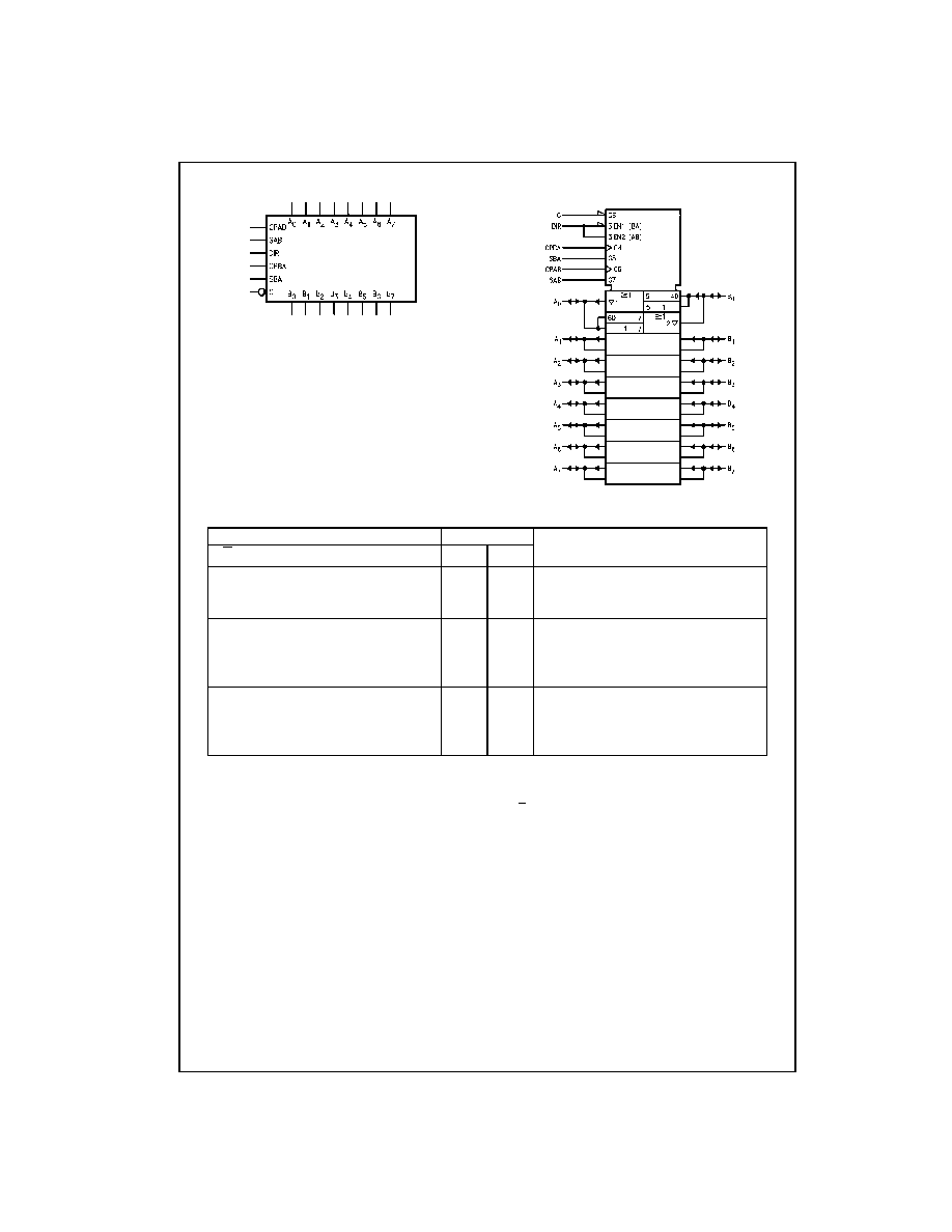
Connection Diagram
Pin Descriptions
FACT
, Quiet Series
, FACT Quiet Series
and GTO
are trademarks of Fairchild Semiconductor Corporation
Order Number
Package Number
Package Description
74ACQ646SC
M24B
24-Lead Small Outline Integrated Circuit (SOIC), JEDEC MS-013, 0.300 Wide
74ACQ464ASPC
N24C
24-Lead Plastic Dual-In-Line Package (PDIP), JEDEC MS-001, 0.300 Wide
74ACTQ646SC
M24B
24-Lead Small Outline Integrated Circuit (SOIC), JEDEC MS-013, 0.300 Wide
74ACTQ464ASPC
N24C
24-Lead Plastic Dual-In-Line Package (PDIP), JEDEC MS-001, 0.300 Wide
Pin Names
Descriptions
A
0
≠A
7
Data Register A Inputs
Data Register A Outputs
B
0
≠B
7
Data Register B Inputs
Data Register B Outputs
CPAB, CPBA
Clock Pulse Inputs
SAB, SBA
Transmit/Receive Inputs
G
Output Enable Input
DIR
Direction Control Input
www.fairchildsemi.com
2
74
A
C
Q646
∑
7
4
AC
T
Q
646
Logic Symbols
IEEE/IEC
Function Table
H
=
HIGH Voltage Level
L
=
LOW Voltage Level
X
=
Immaterial
=
LOW-to-HIGH Transition
Note 1: The data output functions may be enabled or disabled by various signals at the G and DIR inputs. Data input functions are always enabled; i.e., data
at the bus pins will be stored on every LOW-to-HIGH transition of the appropriate clock inputs.
Inputs
Data I/O (Note 1)
Function
G
DIR
CPAB CPBA
SAB
SBA
A
0
≠A
7
B
0
≠B
7
H
X
H or L H or L
X
X
Isolation
H
X
X
X
X
Input
Input
Clock A
n
Data into A Register
H
X
X
X
X
Clock B
n
Data into B Register
L
H
X
X
L
X
A
n
to B
n
--Real Time (Transparent Mode)
L
H
X
L
X
Input
Output Clock A
n
Data into A Register
L
H
H or L
X
H
X
A Register to B
n
(Stored Mode)
L
H
X
H
X
Clock A
n
Data into A Register and Output to B
n
L
L
X
X
X
L
B
n
to A
n
--Real Time (Transparent Mode)
L
L
X
X
L
Output
Input
Clock B
n
Data into B Register
L
L
X
H or L
X
H
B Register to A
n
(Stored Mode)
L
L
X
X
H
Clock B
n
Data into B Register and Output to A
n
3
www.fairchildsemi.com
7
4
AC
Q646
∑
74AC
T
Q
6
4
6
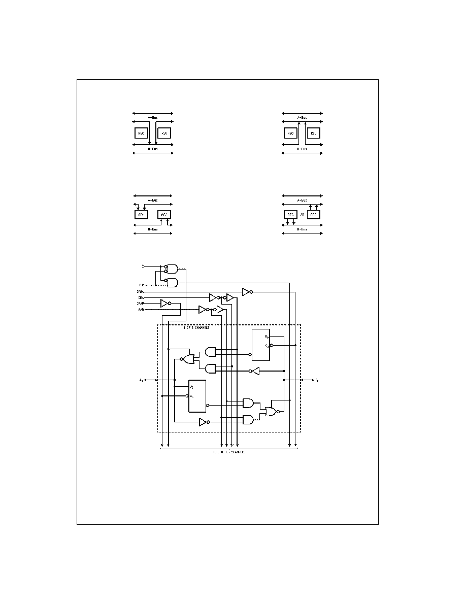
Real Time Transfer
A-Bus to B-Bus
FIGURE 1.
Real Time Transfer
B-Bus to A-Bus
FIGURE 2.
Storage from
Bus to Register
FIGURE 3.
Transfer from
Register to Bus
FIGURE 4.
Logic Diagram
Please note that this diagram is provided only for the understanding of logic operations and should not be used to estimate propagation delays.
www.fairchildsemi.com
4
74
A
C
Q646
∑
7
4
AC
T
Q
646
Absolute Maximum Ratings
(Note 2)
Recommended Operating
Conditions
Note 2: Absolute maximum ratings are those values beyond which damage
to the device may occur. The databook specifications should be met, with-
out exception, to ensure that the system design is reliable over its power
supply, temperature, and output/input loading variables. Fairchild does not
recommend operation of FACT
circuits outside databook specifications.
DC Electrical Characteristics for ACQ
Supply Voltage (V
CC
)
-
0.5V to
+
7.0V
DC Input Diode Current (I
IK
)
V
I
=
-
0.5V
-
20 mA
V
I
=
V
CC
+
0.5V
+
20 mA
DC Input Voltage (V
I
)
-
0.5V to V
CC
+
0.5V
DC Output Diode Current (I
OK
)
V
O
=
-
0.5V
-
20 mA
V
O
=
V
CC
+
0.5V
+
20 mA
DC Output Voltage (V
O
)
-
0.5V to V
CC
+
0.5V
DC Output Source
or Sink Current (I
O
)
±
50 mA
DC V
CC
or Ground Current
per Output Pin (I
CC
or I
GND
)
±
50 mA
Storage Temperature (T
STG
)
-
65
∞
C to
+
150
∞
C
DC Latch-Up Source
or Sink Current
±
300 mA
Junction Temperature (T
J
)
PDIP
140
∞
C
Supply Voltage (V
CC
)
ACQ
2.0V to 6.0V
ACTQ
4.5V to 5.5V
Input Voltage (V
I
)
0V to V
CC
Output Voltage (V
O
)
0V to V
CC
Operating Temperature (T
A
)
-
40
∞
C to
+
85
∞
C
Minimum Input Edge Rate
V/
t
ACQ Devices
V
IN
from 30% to 70% of V
CC
V
CC
@ 3.0V, 4.5V, 5.5V
125 mV/ns
Minimum Input Edge Rate
V/
t
ACTQ Devices
V
IN
from 0.8V to 2.0V
V
CC
@ 4.5V, 5.5V
125 mV/ns
Symbol
Parameter
V
CC
T
A
=
+
25
∞
C
T
A
=
-
40
∞
C to
+
85
∞
C
Units
Conditions
(V)
Typ
Guaranteed Limits
V
IH
Minimum HIGH Level
3.0
1.5
2.1
2.1
V
OUT
=
0.1V
Input Voltage
4.5
2.25
3.15
3.15
V
or V
CC
-
0.1V
5.5
2.75
3.85
3.85
V
IL
Maximum LOW Level
3.0
1.5
0.9
0.9
V
OUT
=
0.1V
Input Voltage
4.5
2.25
1.35
1.35
V
or V
CC
-
0.1V
5.5
2.75
1.65
1.65
V
OH
Minimum HIGH Level
3.0
2.99
2.9
2.9
Output Voltage
4.5
4.49
4.4
4.4
V
I
OUT
=
-
50
µ
A
5.5
5.49
5.4
5.4
V
IN
=
V
IL
or V
IH
3.0
2.56
2.46
I
OH
=
-
12 mA
4.5
3.86
3.76
V
I
OH
=
-
24 mA
5.5
4.85
4.76
I
OH
=
-
24 mA (Note 3)
V
OL
Maximum LOW Level
3.0
0.002
0.1
0.1
Output Voltage
4.5
0.001
0.1
0.1
V
I
OUT
=
50
µ
A
5.5
0.001
0.1
0.1
V
IN
=
V
IL
or V
IH
3.0
0.36
0.44
I
OL
=
12 mA
4.5
0.36
0.44
V
I
OL
=
24 mA
5.5
0.36
0.44
I
OL
=
24 mA (Note 3)
I
IN
(Note 5) Maximum Input Leakage Current
5.5
±
0.1
±
1.0
µ
A
V
I
=
V
CC
, GND
I
OLD
Minimum Dynamic
5.5
75
mA
V
OLD
=
1.65V Max
I
OHD
Output Current (Note 4)
5.5
-
75
mA
V
OHD
=
3.85V Min
I
CC
Maximum Quiescent
5.5
8.0
80.0
µ
A
V
IN
=
V
CC
or GND
(Note 5)
Supply Current
I
OZT
Maximum I/O
V
I
(OE)
=
V
IL
, V
IH
Leakage Current
5.5
±
0.6
±
6.0
µ
A
V
I
=
V
CC
, GND
(A
n
, B
n
Inputs)
V
O
=
V
CC
, GND
V
OLP
Quiet Output
5.0
1.1
1.5
V
Figures 5, 6
Maximum Dynamic V
OL
(Note 6)(Note 7)
5
www.fairchildsemi.com
7
4
AC
Q646
∑
74AC
T
Q
6
4
6
DC Electrical Characteristics for ACQ
(Continued)
Note 3: Maximum of 8 outputs loaded; thresholds on input associated with output under test.
Note 4: Maximum test duration 2.0 ms, one output loaded at a time.
Note 5: I
IN
and I
CC
@ 3.0V are guaranteed to be less than or equal to the respective limit @ 5.5V V
CC
.
Note 6: Plastic DIP package.
Note 7: Max number of outputs defined as (n). Data inputs are driven 0V to 5V. One output @ GND.
Note 8: Max number of Data Inputs (n) switching. (n
-
1) inputs switching 0V to 5V (ACQ). Input-under-test switching 5V to threshold (V
ILD
),
0V to threshold (V
IHD
) f
=
1 MHz.
DC Electrical Characteristics for ACTQ
Note 9: All outputs loaded; thresholds on input associated with output under test.
Note 10: Maximum test duration 2.0 ms, one output loaded at a time.
Note 11: Plastic DIP Package.
Note 12: Max number of outputs defined as (n). Data inputs are driven 0V to 3V. One output @ GND.
Note 13: Max number of data inputs (n) switching. (n
-
1) inputs switching 0V to 3V (ACTQ). Input-under-test switching: 3V to threshold (V
ILD
),
0V to threshold (V
IHD
), f
=
1 MHz.
Symbol
Parameter
V
CC
T
A
=
+
25
∞
C
T
A
=
-
40
∞
C to
+
85
∞
C
Units
Conditions
(V)
Typ
Guaranteed Limits
V
OLV
Quiet Output
5.0
-
0.6
-
1.2
V
Figures 5, 6
Minimum Dynamic V
OL
(Note 6)(Note 7)
V
IHD
Minimum HIGH Level
5.0
3.1
3.5
V
(Note 6)(Note 8)
Dynamic Input Voltage
V
ILD
Maximum LOW Level
5.0
1.9
1.5
V
(Note 6)(Note 8)
Dynamic Input Voltage
Symbol
Parameter
V
CC
T
A
=
+
25
∞
C
T
A
=
-
40
∞
C to
+
85
∞
C
Units
Conditions
(V)
Typ
Guaranteed Limits
V
IH
Minimum HIGH Level
4.5
1.5
2.0
2.0
V
V
OUT
=
0.1V
Input Voltage
5.5
1.5
2.0
2.0
or V
CC
-
0.1V
V
IL
Maximum LOW Level
4.5
1.5
0.8
0.8
V
V
OUT
=
0.1V
Input Voltage
5.5
1.5
0.8
0.8
or V
CC
-
0.1V
V
OH
Minimum HIGH Level
4.5
4.49
4.4
4.4
V
I
OUT
=
-
50
µ
A
Output Voltage
5.5
5.49
5.4
5.4
V
IN
=
V
IL
or V
IH
4.5
3.86
3.76
V
I
OH
=
-
24 mA
5.5
4.86
4.76
I
OH
=
-
24 mA (Note 9)
V
OL
Maximum LOW Level
4.5
0.001
0.1
0.1
V
I
OUT
=
50
µ
A
Output Voltage
5.5
0.001
0.1
0.1
V
IN
=
V
IL
or V
IH
4.5
0.36
0.44
V
I
OL
=
24 mA
5.5
0.36
0.44
I
OL
=
24 mA (Note 9)
I
IN
Maximum Input Leakage Current
5.5
±
0.1
±
1.0
µ
A
V
I
=
V
CC
, GND
I
OZT
Maximum I/O Leakage Current
5.5
±
0.6
±
6.0
µ
A
V
I
=
V
IL
, V
IH
(A
n
, B
n
Inputs)
V
O
=
V
CC
, GND
I
CCT
Maximum I
CC
/Input
5.5
0.6
1.5
mA
V
I
=
V
CC
-
2.1V
I
OLD
Minimum Dynamic
5.5
75
mA
V
OLD
=
1.65V Max
I
OHD
Output Current (Note 10)
5.5
-
75
mA
V
OHD
=
3.85V Min
I
CC
Maximum Quiescent
5.5
8.0
80.0
µ
A
V
IN
=
V
CC
Supply Current
or GND
V
OLP
Quiet Output
5.0
1.1
1.5
V
Figures 5, 6
Maximum Dynamic V
OL
(Note 11)(Note 12)
V
OLV
Quiet Output
5.0
-
0.6
-
1.2
V
Figures 5, 6
Minimum Dynamic V
OL
(Note 11)(Note 12)
V
IHD
Minimum HIGH Level
5.0
1.7
2.0
V
(Note 11)(Note 13)
Dynamic Input Voltage
V
ILD
Maximum LOW Level
5.0
1.2
0.8
V
(Note 11)(Note 13)
Dynamic Input Voltage