
© 2000 Fairchild Semiconductor Corporation
DS010685
www.fairchildsemi.com
March 1990
Revised September 2000
7
4
AC
Q544 ∑ 74AC
T
Q
5
4
4
Qui
e
t Seri
es
Oct
a
l
Regi
ster
ed T
r
anscei
ver
wit
h
3-
ST
A
T
E
Output
s
74ACQ544 ∑ 74ACTQ544
Quiet Series
Octal Registered Transceiver
with 3-STATE Outputs
General Description
The ACQ/ACTQ544 is an inverting octal transceiver con-
taining two sets of D-type registers for temporary storage of
data flowing in either direction. Separate Latch Enable and
Output Enable inputs are provided for each register to per-
mit independent input and output control in either direction
of data flow. The 544 inverts data in both directions.
The ACQ/ACTQ utilizes Fairchild FACT Quiet Series
technology to guarantee quiet output switching and
improved dynamic threshold performance. FACT Quiet
Series features GTO
output control and undershoot cor-
rector in addition to a split ground bus for superior perfor-
mance.
Features
s
Guaranteed simultaneous switching noise level and
dynamic threshold performance
s
Guaranteed pin-to-pin skew AC performance
s
8-bit inverting octal latched transceiver
s
Separate controls for data flow in each direction
s
Back-to-back registers for storage
s
Outputs source/sink 24 mA
Ordering Code:
Device also available in Tape and Reel. Specify by appending suffix letter "X" to the ordering code.
Connection Diagram
Pin Descriptions
FACT
, Quiet Series
, FACT Quiet Series
and GTO
are trademarks of Fairchild Semiconductor Corporation.
Order Number
Package Number
Package Description
74ACQ544SC
M24B
24-Lead Small Outline Integrated Circuit (SOIC), JEDEC MS-013, 0.300 Wide
74ACQ544SPC
N24C
24-Lead Plastic Dual-In-Line Package (PDIP), JEDEC MS-001, 0.300 Wide
74ACTQ544SC
M24B
24-Lead Small Outline Integrated Circuit (SOIC), JEDEC MS-013, 0.300 Wide
74ACTQ544SPC
N24C
24-Lead Plastic Dual-In-Line Package (PDIP), JEDEC MS-001, 0.300 Wide
Pin Names
Description
OEAB
A-to-B Output Enable Input (Active LOW)
OEBA
B-to-A Output Enable Input (Active LOW)
CEAB
A-to-B Enable Input (Active LOW)
CEBA
B-to-A Enable Input (Active LOW)
LEAB
A-to-B Latch Enable Input (Active LOW)
LEBA
B-to-A Latch Enable Input (Active LOW)
A
0
≠A
7
A-to-B Data Inputs or
B-to-A 3-STATE Outputs
B
0
≠B
7
B-to-A Data Inputs or
A-to-B 3-STATE Outputs

www.fairchildsemi.com
2
74
A
C
Q544
∑
7
4
AC
T
Q
544
Logic Symbols
IEEE/IEC
Functional Description
The ACQ/ACTQ544 contains two sets of eight D-type
latches, with separate input and output controls for each
set. For data flow from A to B, for example, the A-to-B
Enable (CEAB) input must be LOW in order to enter data
from A
0
≠A
7
or take data from B
0
≠B
7
, as indicated in the
Data I/O Control Table. With CEAB LOW, a LOW signal on
the A-to-B Latch Enable (LEAB) input makes the A-to-B
latches transparent; a subsequent LOW-to-HIGH transition
of the LEAB signal puts the A latches in the storage mode
and their outputs no longer change with the A inputs. With
CEAB and OEAB both LOW, the 3-STATE B output buffers
are active and reflect the data present at the output of the A
latches. Control of data flow from B to A is similar, but using
the CEBA, LEBA and OEBA inputs.
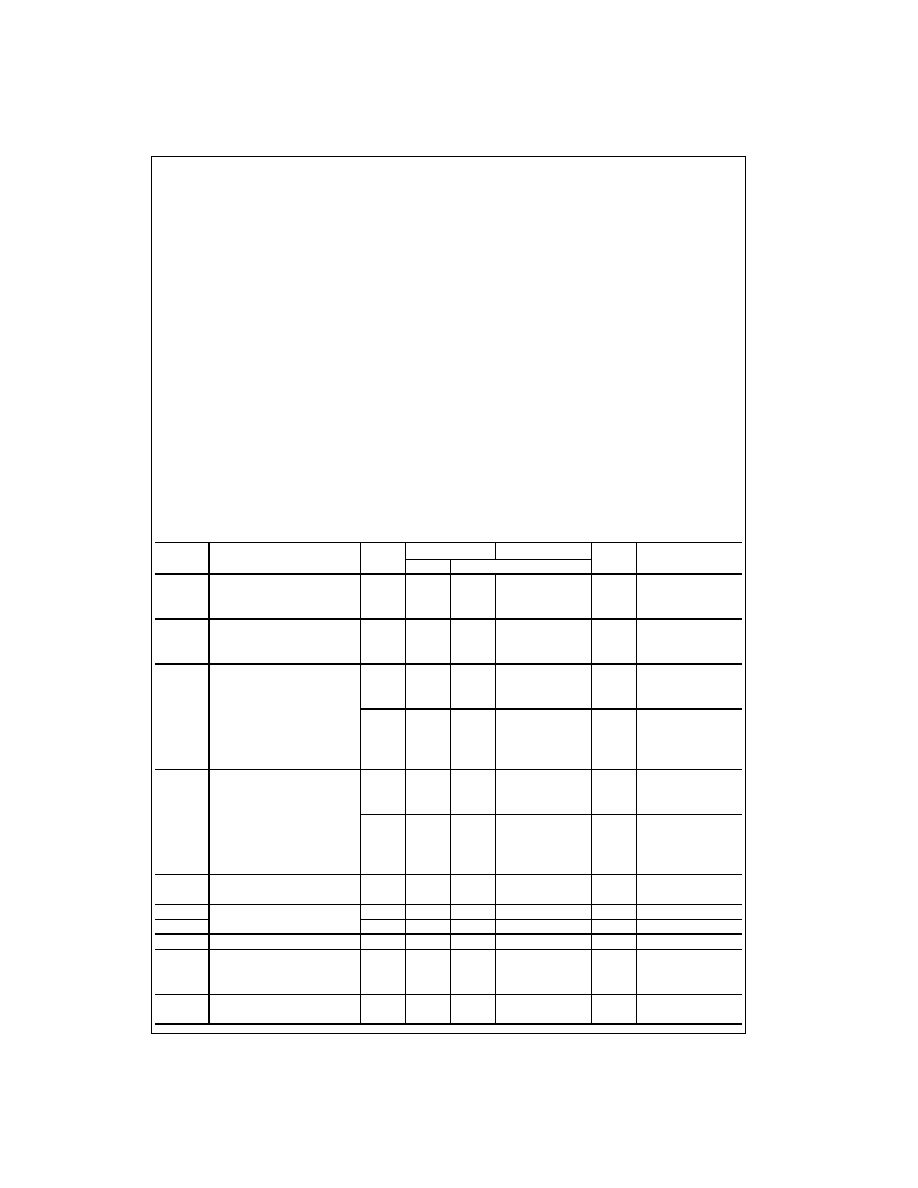
Data I/O Control Table
H
=
HIGH Voltage Level
L
=
LOW Voltage Level
X
=
Immaterial
A-to-B data flow shown; B-to-A flow control is the same, except using
CEBA, LEBA and OEBA
Logic Diagram
Please note that this diagram is provided only for the understanding of logic operations and should not be used to estimate propagation delays.
Inputs
Latch Output
CEAB
LEAB
OEAB
Status
Buffers
H
X
X
Latched
High Z
X
H
X
Latched
--
L
L
X
Transparent
--
X
X
H
--
High Z
L
X
L
--
Driving
3
www.fairchildsemi.com
7
4
AC
Q544
∑
74AC
T
Q
5
4
4
Absolute Maximum Ratings
(Note 1)
Recommended Operating
Conditions
Note 1: Absolute maximum ratings are those values beyond which damage
to the device may occur. The databook specifications should be met, with-
out exception, to ensure that the system design is reliable over its power
supply, temperature, and output/input loading variables. Fairchild does not
recommend operation of FACT
circuits outside databook specifications.
DC Electrical Characteristics for ACQ
Supply Voltage (V
CC
)
-
0.5V to
+
7.0V
DC Input Diode Current (I
IK
)
V
I
=
-
0.5V
-
20 mA
V
I
=
V
CC
+
0.5V
+
20 mA
DC Input Voltage (V
I
)
-
0.5V to V
CC
+
0.5V
DC Output Diode Current (I
OK
)
V
O
=
-
0.5V
-
20 mA
V
O
=
V
CC
+
0.5V
+
20 mA
DC Output Voltage (V
O
)
-
0.5V to V
CC
+
0.5V
DC Output Source
or Sink Current (I
O
)
±
50 mA
DC V
CC
or Ground Current
per Output Pin (I
CC
or I
GND
)
±
50 mA
Storage Temperature (T
STG
)
-
65
∞
C to
+
150
∞
C
DC Latch-up Source or
Sink Current
±
300 mA
Junction Temperature (T
J
)
PDIP
140
∞
C
Supply Voltage V
CC
ACQ
2.0V to 6.0V
ACTQ
4.5V to 5.5V
Input Voltage (V
I
)
0V to V
CC
Output Voltage (V
O
)
0V to V
CC
Operating Temperature (T
A
)
-
40
∞
C to
+
85
∞
C
Minimum Input Edge Rate
V/
t
ACQ Devices
V
IN
from 30% to 70% of V
CC
V
CC
@3.0V, 4.5V, 5.5V
125 mV/ns
Minimum Input Edge Rate
V/
t
ACTQ Devices
V
IN
from 0.8V to 2.0V
V
CC
@ 4.5V, 5.5V
125 mV/ns
Symbol
Parameter
V
CC
T
A
=
+
25
∞
C
T
A
=
-
40
∞
C to
+
85
∞
C
Units
Conditions
(V)
Typ
Guaranteed Limits
V
IH
Minimum HIGH Level
3.0
1.5
2.1
2.1
V
OUT
=
0.1V
Input Voltage
4.5
2.25
3.15
3.15
V
or V
CC
-
0.1V
5.5
2.75
3.85
3.85
V
IL
Maximum LOW Level
3.0
1.5
0.9
0.9
V
OUT
=
0.1V
Input Voltage
4.5
2.25
1.35
1.35
V
or V
CC
-
0.1V
5.5
2.75
1.65
1.65
V
OH
Minimum HIGH Level
3.0
2.99
2.9
2.9
Output Voltage
4.5
4.49
4.4
4.4
V
I
OUT
=
-
50
µ
A
5.5
5.49
5.4
5.4
V
IN
=
V
IL
or V
IH
3.0
2.56
2.46
I
OH
=
-
12 mA
4.5
3.86
3.76
V
I
OH
=
-
24 mA
5.5
4.86
4.76
I
OH
=
-
24 mA (Note 2)
V
OL
Maximum LOW Level
3.0
0.002
0.1
0.1
Output Voltage
4.5
0.001
0.1
0.1
V
I
OUT
=
50
µ
A
5.5
0.001
0.1
0.1
V
IN
=
V
IL
or V
IH
3.0
0.36
0.44
I
OL
=
12 mA
4.5
0.36
0.44
V
I
OL
=
24 mA
5.5
0.36
0.44
I
OL
=
24 mA (Note 2)
I
IN
Maximum Input
5.5
±
0.1
±
1.0
µ
A
V
I
=
V
CC
, GND
(Note 4)
Leakage Current
I
OLD
Minimum Dynamic
5.5
75
mA
V
OLD
=
1.65V Max
I
OHD
Output Current (Note 3)
5.5
-
75
mA
V
OHD
=
3.85V Min
I
CC
(Note 4) Maximum Quiescent Supply Current
5.5
8.0
80.0
µ
A
V
IN
=
V
CC
or GND
I
OZT
Maximum I/O
V
I
(OE)
=
V
IL
, V
IH
Leakage Current
5.5
±
0.6
±
6.0
µ
A
V
I
=
V
CC
, GND
V
O
=
V
CC
, GND
V
OLP
Quiet Output
5.0
1.1
1.5
V
Figures 1, 2
Maximum Dynamic V
OL
(Note 5)(Note 6)
www.fairchildsemi.com
4
74
A
C
Q544
∑
7
4
AC
T
Q
544
DC Electrical Characteristics for ACQ
(Continued)
Note 2: All outputs loaded; thresholds on input associated with output under test.
Note 3: Maximum test duration 2.0 ms, one output loaded at a time.
Note 4: I
IN
and I
CC
@ 3.0V are guaranteed to be less than or equal to the respective limit @ 5.5V V
CC
.
Note 5: DIP package.
Note 6: Max number of outputs defined as (n). Data Inputs are driven 0V to 5V. One output @ GND.
Note 7: Max number of Data Inputs (n) switching. (n-1) inputs switching 0V to 5V (ACQ). Input-under-test switching: 5V to threshold (V
ILD
),
0V to threshold (V
IHD
). f
=
1 MHz.
DC Electrical Characteristics for ACTQ
Note 8: All outputs loaded; thresholds on input associated with output under test.
Note 9: Maximum test duration 2.0 ms, one output loaded at a time.
Note 10: DIP package.
Note 11: Max number of outputs defined as (n-1). Data Inputs are driven 0V to 3V, one output @ GND.
Note 12: Max number of Data Inputs (n) switching (n-1) inputs switching 0V to 3V (ACTQ). Input-under-test switching:
3V to threshold (V
ILD
), 0V to threshold (V
IHD
), f
=
1 MHz.
Symbol
Parameter
V
CC
T
A
=
+
25
∞
C
T
A
=
-
40
∞
C to
+
85
∞
C
Units
Conditions
(V)
Typ
Guaranteed Limits
V
OLV
Quiet Output
5.0
-
0.6
-
1.2
V
Figures 1, 2
Minimum Dynamic V
OL
(Note 5)(Note 6)
V
IHD
Minimum HIGH Level
5.0
3.1
3.5
V
(Note 5)(Note 7)
Dynamic Input Voltage
V
ILD
Maximum LOW Level
5.0
1.9
1.5
V
(Note 5)(Note 7)
Dynamic Input Voltage
Symbol
Parameter
V
CC
T
A
=
+
25
∞
C
T
A
=
-
40
∞
C to
+
85
∞
C
Units
Conditions
(V)
Typ
Guaranteed Limits
V
IH
Minimum HIGH Level
4.5
1.5
2.0
2.0
V
V
OUT
=
0.1V
Input Voltage
5.5
1.5
2.0
2.0
or V
CC
-
0.1V
V
IL
Maximum LOW Level
4.5
1.5
0.8
0.8
V
V
OUT
=
0.1V
Input Voltage
5.5
1.5
0.8
0.8
or V
CC
-
0.1V
V
OH
Minimum HIGH Level
4.5
4.49
4.4
4.4
V
I
OUT
=
-
50
µ
A
Output Voltage
5.5
5.49
5.4
5.4
V
IN
=
V
IL
or V
IH
4.5
3.86
3.76
V
I
OH
=
-
24 mA
5.5
4.86
4.76
I
OH
=
-
24 mA (Note 8)
V
OL
Maximum LOW Level
4.5
0.001
0.1
0.1
V
I
OUT
=
50
µ
A
Output Voltage
5.5
0.001
0.1
0.1
V
IN
=
V
IL
or V
IH
4.5
0.36
0.44
V
I
OL
=
24 mA
5.5
0.36
0.44
I
OL
=
24 mA (Note 8)
I
IN
Maximum Input Leakage Current
5.5
±
0.1
±
1.0
µ
A
V
I
=
V
CC
, GND
I
OZT
Maximum I/O
5.5
±
0.6
±
6.0
µ
A
V
I
, (OE)
=
V
IL
, V
IH
Leakage Current
V
O
=
V
CC
, GND
I
CCT
Maximum I
CC
/Input
5.5
0.6
1.5
mA
V
I
=
V
CC
-
2.1V
I
OLD
Minimum Dynamic
5.5
75
mA
V
OLD
=
1.65V Max
I
OHD
Output Current (Note 9)
5.5
-
75
mA
V
OHD
=
3.85V Min
I
CC
Maximum Quiescent or GND
5.5
8.0
80.0
µ
A
V
IN
=
V
CC
V
OLP
Quiet Output
5.0
1.1
1.5
V
Figure 1, Figure 2
Maximum Dynamic V
OL
(Note 10)(Note 11)
V
OLV
Quiet Output
5.0
-
0.6
-
1.2
V
Figure 1, Figure 2
Minimum Dynamic V
OL
(Note 10)(Note 11)
V
IHD
Maximum HIGH Level
5.0
1.9
2.2
V
(Note 10)(Note 12)
Dynamic Input Voltage
V
ILD
Maximum LOW Level
5.0
1.2
0.8
V
(Note 10)(Note 12)
Dynamic Input Voltage

5
www.fairchildsemi.com
7
4
AC
Q544
∑
74AC
T
Q
5
4
4
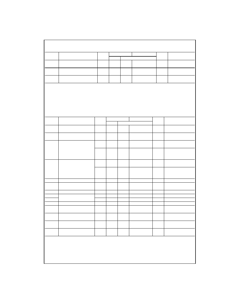
AC Electrical Characteristics for ACQ
Note 13: Voltage Range 5.0 is 5.0V
±
0.5V
Voltage Range 3.3 is 3.3V
±
0.3V
Note 14: Skew is defined as the absolute value of the difference between the actual propagation delay for any two outputs within the same packaged device.
The specification applies to any outputs switching in the same direction, either HIGH-to-LOW (t
OSHL
) or LOW-to-HIGH (t
OSLH
). Parameter guaranteed by
design. Not tested.
AC Operating Requirements for ACQ
Note 15: Voltage Range 5.0 is 5.0V
±
0.5V
Voltage Range 3.3 is 3.0V
±
0.3V
V
CC
T
A
=
+
25
∞
C
T
A
=
-
40
∞
C to
+
85
∞
C
Symbol
Parameter
(V)
C
L
=
50 pF
C
L
=
50 pF
Units
(Note 13)
Min
Typ
Max
Min
Max
t
PLH
Propagation Delay
3.3
1.5
8.0
11.0
1.5
12.0
t
PHL
Transparent Mode
5.0
1.5
5.0
7.5
1.5
8.0
ns
A
n
to B
n
or B
n
to A
n
t
PLH
Propagation Delay
3.3
1.5
8.5
12.0
1.5
12.5
ns
t
PHL
LEBA, LEAB to A
n
, B
n
5.0
1.5
6.0
8.0
1.5
8.5
Output Enable Time
3.3
1.5
10.0
14.0
1.5
15.0
t
PZH
OEBA or OEAB to A
n
or B
n
5.0
1.5
7.0
9.5
1.5
10.0
ns
t
PZL
CEBA or CEAB to A
n
or B
n
Output Disable Time
3.3
1.0
7.5
10.5
1.0
11.0
t
PHZ
OEBA or OEAB to A
n
or B
n
5.0
1.0
5.0
7.0
1.0
7.5
ns
t
PLZ
CEBA or CEAB to A
n
or B
n
t
OSHL
Output to Output
3.3
1.0
1.5
1.5
ns
t
OSLH
Skew (Note 14)
5.0
0.5
1.0
1.0
V
CC
T
A
=
+
25
∞
C
T
A
=
-
40
∞
C to
+
85
∞
C
Symbol
Parameter
(V)
C
L
=
50 pF
C
L
=
50 pF
Units
(Note 15)
Typ
Guaranteed Minimum
t
S
Setup Time, HIGH or LOW
3.3
3.0
3.0
ns
A
n
or B
n
to LEBA or LEAB
5.0
t
H
Hold Time, HIGH or LOW
3.3
1.5
1.5
ns
A
n
or B
n
to LEBA or LEAB
5.0
t
W
Latch Enable, B to A
3.3
4.0
4.0
ns
Pulse Width, LOW
5.0