© 2005 Fairchild Semiconductor Corporation
DS500677
www.fairchildsemi.com
October 2001
Revised May 2005
7
4
AL
VC1624
4
Low V
o
l
t
age 16-
B
i
t Buff
er/
L
i
ne
Dr
iver
wi
th 3.6V T
o
ler
ant
I
nput
s and
Out
put
s
74ALVC16244
Low Voltage 16-Bit Buffer/Line Driver
with 3.6V Tolerant Inputs and Outputs
General Description
The ALVC16244 contains sixteen non-inverting buffers with
3-STATE outputs to be employed as a memory and
address driver, clock driver, or bus oriented transmitter/
receiver. The device is nibble (4-bit) controlled. Each nibble
has separate 3-STATE control inputs which can be shorted
together for full 16-bit operation.
The 74ALVC16244 is designed for low voltage (1.65V to
3.6V) V
CC
applications with I/O capability up to 3.6V.
The 74ALVC16244 is fabricated with an advanced CMOS
technology to achieve high speed operation while maintain-
ing low CMOS power dissipation.
Features
s
1.65V≠3.6V V
CC
supply operation
s
3.6V tolerant inputs and outputs
s
t
PD
3.0 ns max for 3.0V to 3.6V V
CC
3.5 ns max for 2.3V to 2.7V V
CC
6.0 ns max for 1.65V to 1.95V V
CC
s
Power-off high impedance inputs and outputs
s
Supports live insertion and withdrawal (Note 1)
s
Uses patented noise/EMI reduction circuitry
s
Latch-up conforms to JEDEC JED98
s
ESD performance:
Human body model
!
2000V
Machine model
!
200V
s
Also packaged in plastic Fine-Pitch Ball Grid Array
(FBGA)
Note 1: To ensure the high-impedance state during power up or power
down, OE should be tied to V
CC
through a pull-up resistor; the minimum
value of the resistor is determined by the current-sourcing capability of the
driver.
Ordering Code:
Note 2: BGA package available in Tape and Reel only.
Note 3: Devices also available in Tape and Reel. Specify by appending the suffix letter "X" to the ordering code.
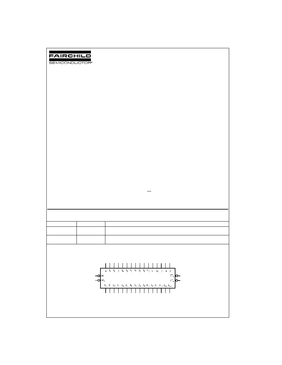
Logic Symbol
Order Number
Package Number
Package Description
74ALVC16244GX
(Note 2)
BGA54A
54-Ball Fine-Pitch Ball Grid Array (FBGA), JEDEC MO-205, 5.5mm Wide
[Tape and Reel]
74ALVC16244MTD
(Note 3)
MTD48
48-Lead Thin Shrink Small Outline Package (TSSOP), JEDEC MO-153, 6.1mm Wide
www.fairchildsemi.com
2
74
A
L
VC16244
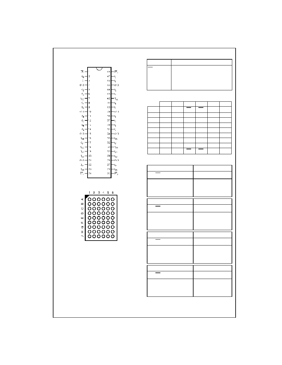
Connection Diagrams
Pin Assignment for TSSOP
Pin Assignment for FBGA
(Top Thru View)
Pin Descriptions
FBGA Pin Assignments
Truth Tables
H
HIGH Voltage Level
L
LOW Voltage Level
X
Immaterial (HIGH or LOW, inputs may not float)
Z
High Impedance
Pin Names
Description
OE
n
Output Enable Input (Active LOW)
I
0
≠I
15
Inputs
O
0
≠O
15
Outputs
NC
No Connect
1
2
3
4
5
6
A
O
0
NC
OE
1
OE
2
NC
I
0
B
O
2
O
1
NC
NC
I
1
I
2
C
O
4
O
3
V
CC
V
CC
I
3
I
4
D
O
6
O
5
GND
GND
I
5
I
6
E
O
8
O
7
GND
GND
I
7
I
8
F
O
10
O
9
GND
GND
I
9
I
10
G
O
12
O
11
V
CC
V
CC
I
11
I
12
H
O
14
O
13
NC
NC
I
13
I
14
J
O
15
NC
OE
4
OE
3
NC
I
15
Inputs
Outputs
OE
1
I
0
≠I
3
O
0
≠O
3
L
L
L
L
H
H
H
X
Z
Inputs
Outputs
OE
3
I
8
-I
11
O
8
≠O
11
L
L
L
L
H
H
H
X
Z
Inputs
Outputs
OE
2
I
4
-I
7
O
4
-O
7
L
L
L
L
H
H
H
X
Z
Inputs
Outputs
OE
4
I
12
-I
15
O
12
-O
15
L
L
L
L
H
H
H
X
Z
3
www.fairchildsemi.com
7
4
AL
VC1624
4
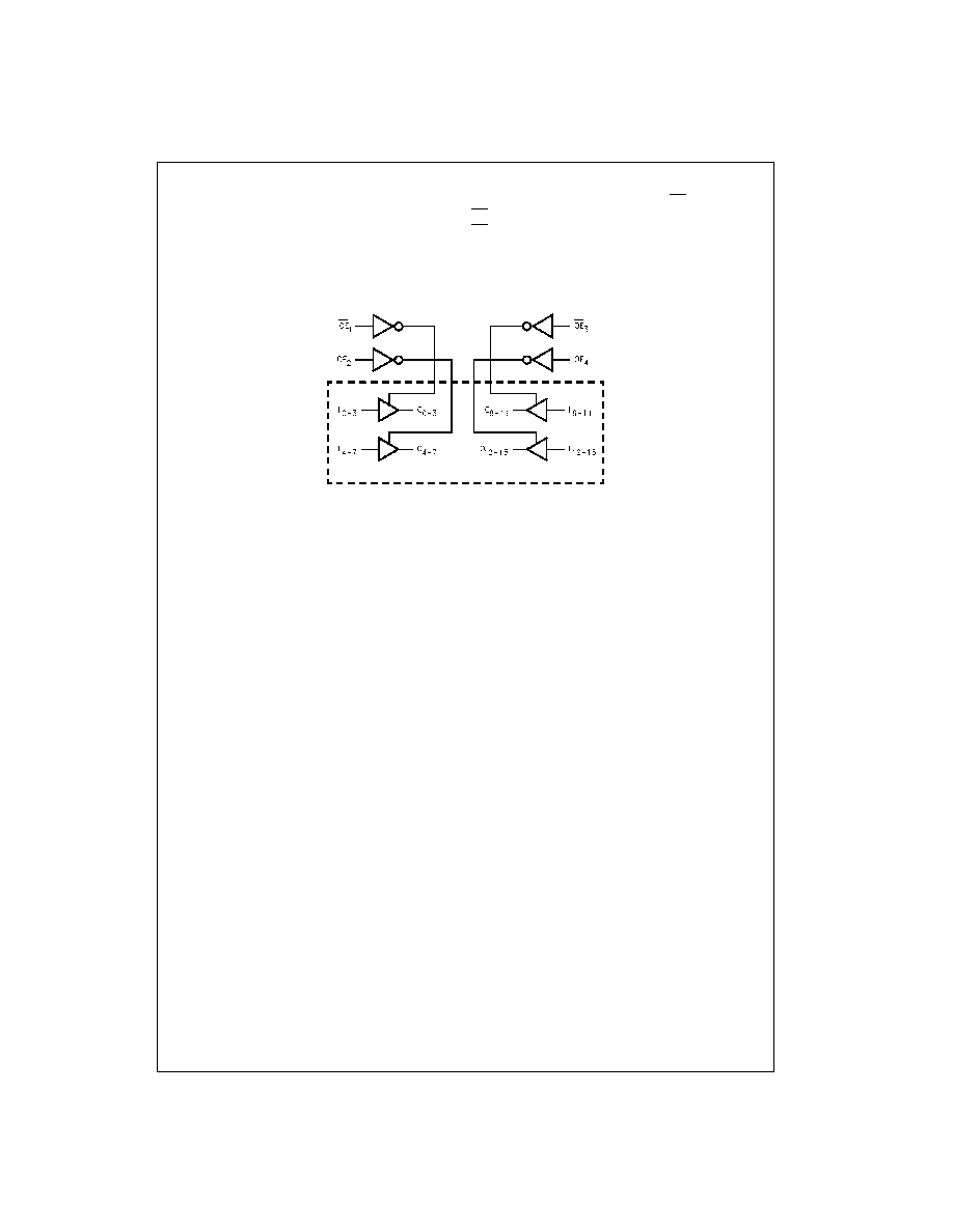
Functional Description
The 74ALVC16244 contains sixteen non-inverting buffers
with 3-STATE outputs. The device is nibble (4 bits) con-
trolled with each nibble functioning identically, but indepen-
dent of each other. The control pins may be shorted
together to obtain full 16-bit operation.The 3-STATE out-
puts are controlled by an Output Enable (OE
n
) input. When
OE
n
is LOW, the outputs are in the 2-state mode. When
OE
n
is HIGH, the standard outputs are in the high imped-
ance mode but this does not interfere with entering new
data into the inputs.
Logic Diagram
www.fairchildsemi.com
4
74
A
L
VC16244
Absolute Maximum Ratings
(Note 4)
Recommended Operating
Conditions
(Note 6)
Note 4: The Absolute Maximum Ratings are those values beyond which
the safety of the device cannot be guaranteed. The device should not be
operated at these limits. The parametric values defined in the Electrical
Characteristics tables are not guaranteed at the Absolute Maximum Rat-
ings. The "Recommended Operating Conditions" table will define the condi-
tions for actual device operation.
Note 5: I
O
Absolute Maximum Rating must be observed, limited to 4.6V.
Note 6: Floating or unused control inputs must be held HIGH or LOW.
DC Electrical Characteristics
Supply Voltage (V
CC
)
0.5V to
4.6V
DC Input Voltage (V
I
)
0.5V to 4.6V
Output Voltage (V
O
) (Note 5)
0.5V to V
CC
0.5V
DC Input Diode Current (I
IK
)
V
I
0V
50 mA
DC Output Diode Current (I
OK
)
V
O
0V
50 mA
DC Output Source/Sink Current
(I
OH
/I
OL
)
r
50 mA
DC V
CC
or GND Current per
Supply Pin (I
CC
or GND)
r
100 mA
Storage Temperature Range (T
STG
)
65
q
C to
150
q
C
Power Supply
Operating
1.65V to 3.6V
Input Voltage (V
I
)
0V to V
CC
Output Voltage (V
O
)
0V to V
CC
Free Air Operating Temperature (T
A
)
40
q
C to
85
q
C
Minimum Input Edge Rate (
'
t/
'
V)
V
IN
0.8V to 2.0V, V
CC
3.0V
10 ns/V
Symbol
Parameter
Conditions
V
CC
Min
Max
Units
(V)
V
IH
HIGH Level Input Voltage
1.65 - 1.95
0.65 x V
CC
V
2.3 - 2.7
1.7
2.7 - 3.6
2.0
V
IL
LOW Level Input Voltage
1.65 - 1.95
0.35 x V
CC
V
2.3 - 2.7
0.7
2.7 - 3.6
0.8
V
OH
HIGH Level Output Voltage
I
OH
100
P
A
1.65 - 3.6
V
CC
- 0.2
V
I
OH
4 mA
1.65
1.2
I
OH
6 mA
2.3
2.0
I
OH
12 mA
2.3
1.7
2.7
2.2
3.0
2.4
I
OH
24 mA
3.0
2
V
OL
LOW Level Output Voltage
I
OL
100
P
A
1.65 - 3.6
0.2
V
I
OL
4 mA
1.65
0.45
I
OL
6 mA
2.3
0.4
I
OL
12 mA
2.3
0.7
2.7
0.4
I
OL
24 mA
3.0
0.55
I
I
Input Leakage Current
0
d
V
I
d
3.6V
3.6
r
5.0
P
A
I
OZ
3-STATE Output Leakage
0
d
V
O
d
3.6V
3.6
r
10
P
A
I
CC
Quiescent Supply Current
V
I
V
CC
or GND, I
O
0
3.6
40
P
A
'
I
CC
Increase in I
CC
per Input
V
IH
V
CC
0.6V
3 - 3.6
750
P
A

5
www.fairchildsemi.com
7
4
AL
VC1624
4
AC Electrical Characteristics
Capacitance
Symbol
Parameter
T
A
40
q
C to
85
q
C, R
L
500
:
Units
C
L
50 pF
C
L
30 pF
V
CC
3.3V
r
0.3V
V
CC
2.7V
V
CC
2.5V
r
0.2V
V
CC
1.8V
r
0.15V
Min
Max
Min
Max
Min
Max
Min
Max
t
PHL
, t
PLH
Propagation Delay
1.3
3
1.5
3.5
1.0
3.0
1.5
6.0
ns
t
PZL
, t
PZH
Output Enable Time
1.3
4.0
1.5
4.6
1.0
4.1
1.5
8.2
ns
t
PLZ
, t
PHZ
Output Disable Time
1.3
4.0
1.5
4.3
1.0
3.8
1.5
6.8
ns
Symbol
Parameter
Conditions
T
A
25
q
C
Units
V
CC
Typical
C
IN
Input Capacitance
V
I
0V or V
CC
3.3
6
pF
C
OUT
Output Capacitance
V
I
0V or V
CC
3.3
7
pF
C
PD
Power Dissipation Capacitance
Outputs Enabled f
10 MHz, C
L
0 pF
3.3
20
pF
2.5
20
www.fairchildsemi.com
6
74
A
L
VC16244
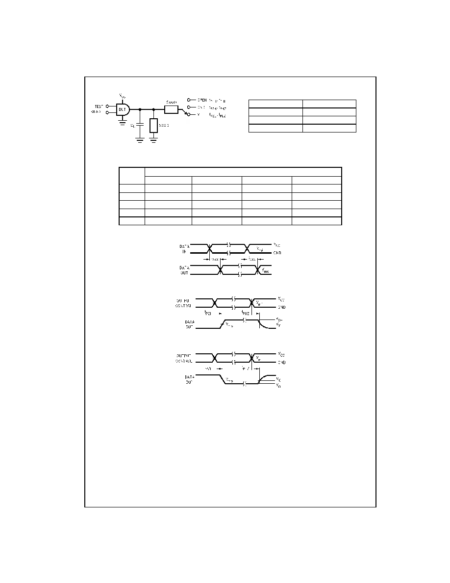
AC Loading and Waveforms
FIGURE 1. AC Test Circuit
Table 1: Values for Figure 1
Table 2: Variable Matrix
(Input Characteristics: f = 1MHz; t
r
= t
f
= 2ns; Z
0
= 50
:
)
FIGURE 2. Waveform for Inverting and Non-Inverting Functions
FIGURE 3. 3-STATE Output High Enable and Disable Times for Low Voltage Logic
FIGURE 4. 3-STATE Output Low Enable and Disable Times for Low Voltage Logic
TEST
SWITCH
t
PLH
, t
PHL
Open
t
PZL
, t
PLZ
V
L
t
PZH
, t
PHZ
GND
Symbol
V
CC
3.3V
r
0.3V
2.7V
2.5V
r
0.2V
1.8V
r
0.15V
V
mi
1.5V
1.5V
V
CC
/2
V
CC
/2
V
mo
1.5V
1.5V
V
CC
/2
V
CC
/2
V
X
V
OL
0.3V
V
OL
0.3V
V
OL
0.15V
V
OL
0.15V
V
Y
V
OH
0.3V
V
OH
0.3V
V
OH
0.15V
V
OH
0.15V
V
L
6V
6V
V
CC
*2
V
CC
*2
7
www.fairchildsemi.com
7
4
AL
VC1624
4
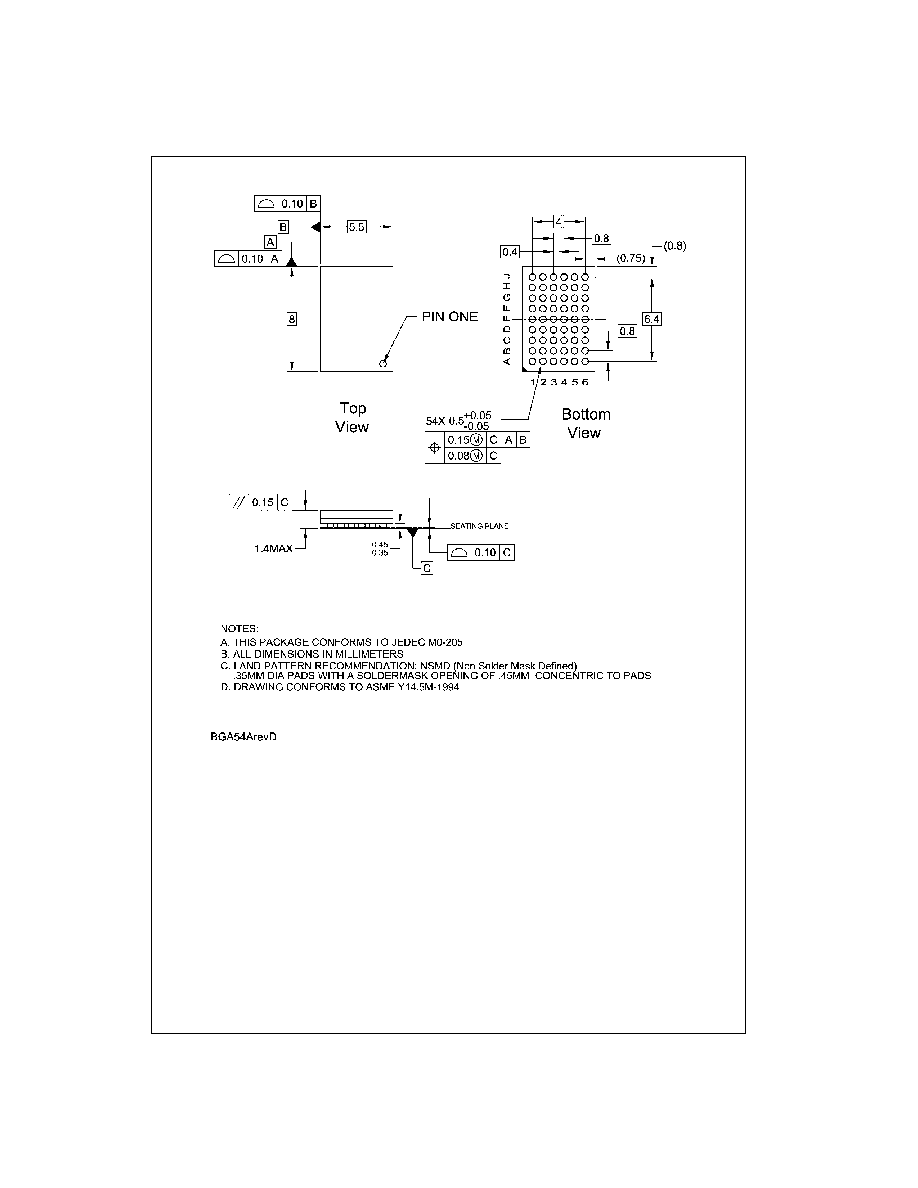
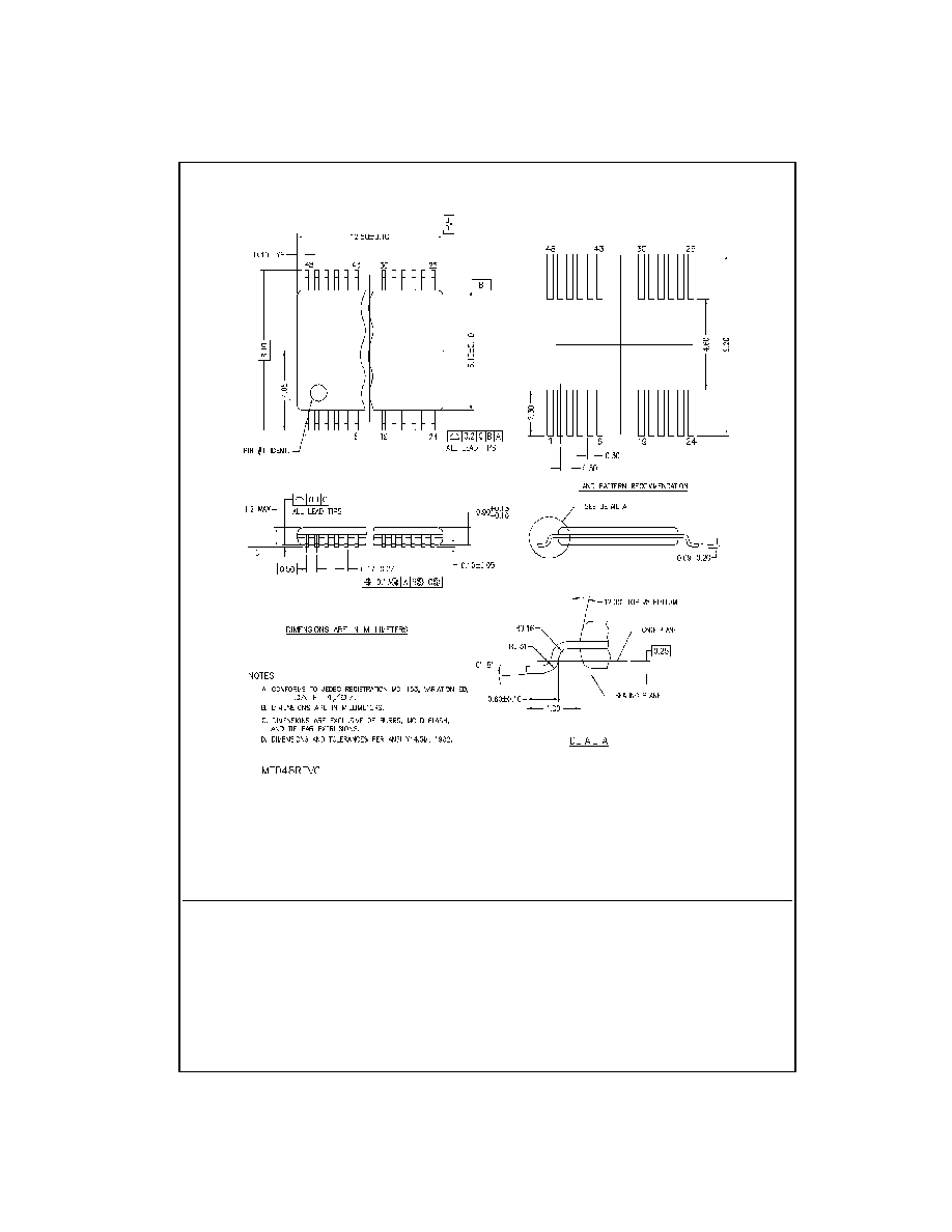
Physical Dimensions
inches (millimeters) unless otherwise noted
54-Ball Fine-Pitch Ball Grid Array (FBGA), JEDEC MO-205, 5.5mm Wide
Package Number BGA54A
www.fairchildsemi.com
8
74AL
VC16244 Low
V
o
l
t
age
1
6
-Bi
t
Buff
er/
L
ine Dri
ver wit
h
3.
6V T
o
l
e
r
ant Input
s
and Output
s
Physical Dimensions
inches (millimeters) unless otherwise noted (Continued)
48-Lead Thin Shrink Small Outline Package (TSSOP), JEDEC MO-153, 6.1mm Wide
Package Number MTD48
Fairchild does not assume any responsibility for use of any circuitry described, no circuit patent licenses are implied and
Fairchild reserves the right at any time without notice to change said circuitry and specifications.
LIFE SUPPORT POLICY
FAIRCHILD'S PRODUCTS ARE NOT AUTHORIZED FOR USE AS CRITICAL COMPONENTS IN LIFE SUPPORT
DEVICES OR SYSTEMS WITHOUT THE EXPRESS WRITTEN APPROVAL OF THE PRESIDENT OF FAIRCHILD
SEMICONDUCTOR CORPORATION. As used herein:
1. Life support devices or systems are devices or systems
which, (a) are intended for surgical implant into the
body, or (b) support or sustain life, and (c) whose failure
to perform when properly used in accordance with
instructions for use provided in the labeling, can be rea-
sonably expected to result in a significant injury to the
user.
2. A critical component in any component of a life support
device or system whose failure to perform can be rea-
sonably expected to cause the failure of the life support
device or system, or to affect its safety or effectiveness.
www.fairchildsemi.com