
© 2005 Fairchild Semiconductor Corporation
DS500687
www.fairchildsemi.com
October 2001
Revised May 2005
7
4
AL
VC1637
3 Low
V
o
l
t
age
16-
B
i
t
T
r
ansp
ar
ent
Lat
ch wi
th
3.
6V T
o
l
e
rant
I
nput
s
and Out
put
s
74ALVC16373
Low Voltage 16-Bit Transparent Latch
with 3.6V Tolerant Inputs and Outputs
General Description
The ALVC16373 contains sixteen non-inverting latches
with 3-STATE outputs and is intended for bus oriented
applications. The device is byte controlled. The flip-flops
appear to be transparent to the data when the Latch
Enable (LE) is HIGH. When LE is LOW, the data that meets
the setup time is latched. Data appears on the bus when
the Output Enable (OE) is LOW. When OE is HIGH, the
outputs are in a high impedance state.
The 74ALVC16373 is designed for low voltage (1.1V to
3.6V) V
CC
applications with I/O compatibility up to 3.6V.
The 74ALVC16373 is fabricated with an advanced CMOS
technology to achieve high speed operation while maintain-
ing low CMOS power dissipation.
Features
s
1.1V to 3.6V V
CC
supply operation
s
3.6V tolerant inputs and outputs
s
t
PD
(I
n
to O
n
)
3.5 ns max for 3.0V to 3.6V V
CC
3.9 ns max for 2.3V to 2.7V V
CC
6.8 ns max for 1.65V to 1.95V V
CC
s
Power-off high impedance inputs and outputs
s
Support live insertion and withdrawal (Note 1)
s
Uses patented noise/EMI reduction circuitry
s
Latchup conforms to JEDEC JED78
s
ESD performance:
Human body model
!
2000V
Machine model
!
200V
s
Also packaged in plastic Fine-Pitch Ball Grid Array
(FBGA) (Preliminary)
Note 1: To ensure the high-impedance state during power up or power
down, OE should be tied to V
CC
through a pull-up resistor; the minimum
value of the resistor is determined by the current-sourcing capability of the
driver.
Ordering Code:
Note 2: BGA package available in Tape and Reel only.
Note 3: Devices also available in Tape and Reel. Specify by appending suffix letter "X" to the ordering code.
Logic Symbol
Order Number
Package Number
Package Description
74ALVC16373GX
(Note 2)
BGA54A
(Preliminary)
54-Ball Fine-Pitch Ball Grid Array (FBGA), JEDEC MO-205, 5.5mm Wide
[TAPE and REEL]
74ALVC16373MTD
(Note 3)
MTD48
48-Lead Thin Shrink Small Outline Package (TSSOP), JEDEC MO-153, 6.1mm Wide
www.fairchildsemi.com
2
74
A
L
VC16373
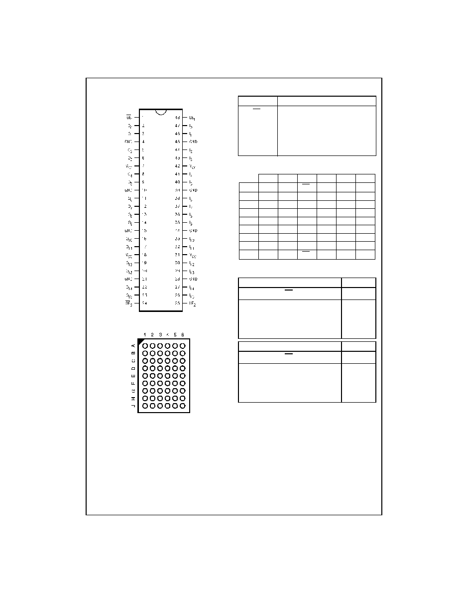
Connection Diagrams
Pin Assignment for TSSOP
Pin Assignment for FBGA
(Top Thru View)
Pin Descriptions
FBGA Pin Assignments
Truth Tables
H
HIGH Voltage Level
L
LOW Voltage Level
X
Immaterial (HIGH or LOW, inputs may not float)
Z
High Impedance
O
0
Previous O
0
before HIGH-to-LOW of Latch Enable
Pin Names
Description
OE
n
Output Enable Input (Active LOW)
LE
n
Latch Enable Input
I
0
≠I
15
Inputs
O
0
≠O
15
Outputs
NC
No Connect
1
2
3
4
5
6
A
O
0
NC
OE
1
LE
1
NC
I
0
B
O
2
O
1
NC
NC
I
1
I
2
C
O
4
O
3
V
CC
V
CC
I
3
I
4
D
O
6
O
5
GND
GND
I
5
I
6
E
O
8
O
7
GND
GND
I
7
I
8
F
O
10
O
9
GND
GND
I
9
I
10
G
O
12
O
11
V
CC
V
CC
I
11
I
12
H
O
14
O
13
NC
NC
I
13
I
14
J
O
15
NC
OE
2
LE
2
NC
I
15
Inputs
Outputs
LE
1
OE
1
I
0
≠I
7
O
0
≠O
7
X
H
X
Z
H
L
L
L
H
L
H
H
L
L
X
O
0
Inputs
Outputs
LE
2
OE
2
I
8
≠I
15
O
8
≠O
15
X
H
X
Z
H
L
L
L
H
L
H
H
L
L
X
O
0
3
www.fairchildsemi.com
7
4
AL
VC1637
3
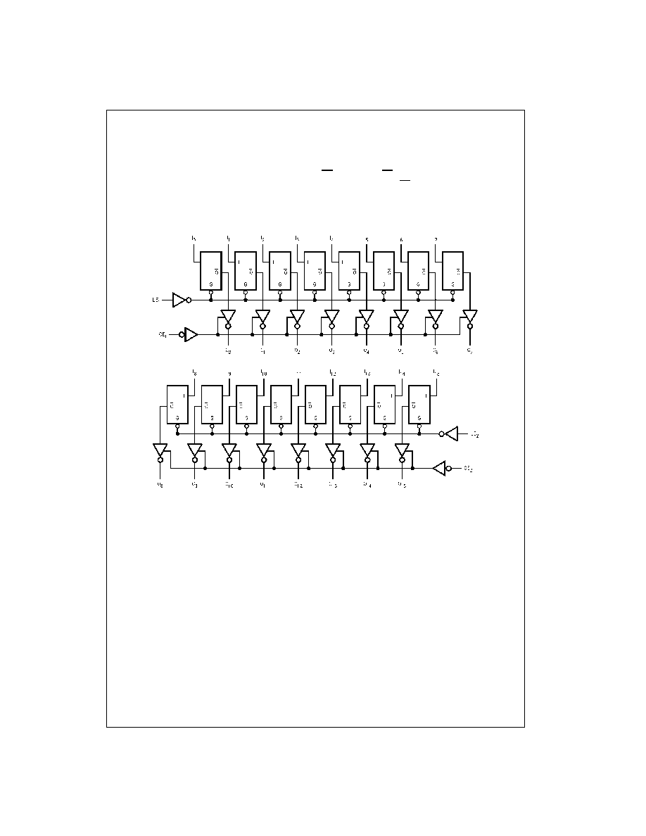
Functional Description
The 74ALVC16373 contains sixteen edge D-type latches
with 3-STATE outputs. The device is byte controlled with
each byte functioning identically, but independent of the
other. Control pins can be shorted together to obtain full
16-bit operation. The following description applies to each
byte. When the Latch Enable (LE
n
) input is HIGH, data on
the I
n
enters the latches. In this condition the latches are
transparent, i.e., a latch output will change state each time
its I input changes. When LE
n
is LOW, the latches store
information that was present on the I inputs a setup time
preceding the HIGH-to-LOW transition on LE
n
. The
3-STATE outputs are controlled by the Output Enable
(OE
n
) input. When OE
n
is LOW the standard outputs are in
the 2-state mode. When OE
n
is HIGH, the standard outputs
are in the high impedance mode but this does not interfere
with entering new data into the latches.
Logic Diagram
Please note that this diagram is provided only for the understanding of logic operations and should not be used to estimate propagation delays.
www.fairchildsemi.com
4
74
A
L
VC16373
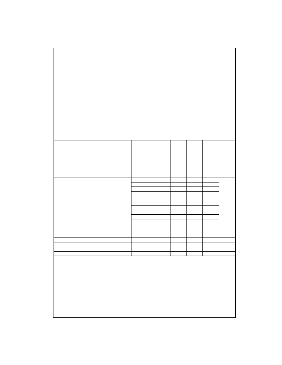
Absolute Maximum Ratings
(Note 4)
Recommended Operating
Conditions
(Note 6)
Note 4: The Absolute Maximum Ratings are those values beyond which
the safety of the device cannot be guaranteed. The device should not be
operated at these limits. The parametric values defined in the Electrical
Characteristics tables are not guaranteed at the Absolute Maximum Rat-
ings. The "Recommended Operating Conditions" table will define the condi-
tions for actual device operation.
Note 5: I
O
Absolute Maximum Rating must be observed.
Note 6: Floating or unused inputs must be held HIGH or LOW.
DC Electrical Characteristics
Supply Voltage (V
CC
)
0.5V to
4.6V
DC Input Voltage (V
I
)
0.5V to 4.6V
Output Voltage (V
O
) (Note 5)
0.5V to V
CC
0.5V
DC Input Diode Current (I
IK
)
V
I
0V
50 mA
DC Output Diode Current (I
OK
)
V
O
0V
50 mA
DC Output Source/Sink Current
(I
OH
/I
OL
)
r
50 mA
DC V
CC
or GND Current per
Supply Pin (I
CC
or GND)
r
100 mA
Storage Temperature Range (T
STG
)
65
q
C to
150
q
C
Power Supply
Operating 1.65V
to
3.6V
Input Voltage (V
I
)
0V to V
CC
Output Voltage (V
O
)
0V to V
CC
Free Air Operating Temperature (T
A
)
40
q
C to
85
q
C
Minimum Input Edge Rate (
'
t/
'
V)
V
IN
0.8V to 2.0V, V
CC
3.0V
10 ns/V
Symbol
Parameter
Conditions
V
CC
Min
Max
Units
(V)
V
IH
HIGH Level Input Voltage
1.65 -1.95
0.65 x V
CC
V
2.3 - 2.7
1.7
2.7 - 3.6
2.0
V
IL
LOW Level Input Voltage
1.65 -1.95
0.35 x V
CC
V
2.3 - 2.7
0.7
2.7 - 3.6
0.8
V
OH
HIGH Level Output Voltage
I
OH
100
P
A
1.65 - 3.6
V
CC
- 0.2
V
I
OH
4 mA
1.65
1.2
I
OH
6 mA
2.3
2
I
OH
12 mA
2.3
1.7
2.7
2.2
3.0
2.4
I
OH
24 mA
3.0
2
V
OL
LOW Level Output Voltage
I
OL
100
P
A
1.65 - 3.6
0.2
V
I
OL
4 mA
1.65
0.45
I
OL
6 mA
2.3
0.4
I
OL
12mA
2.3
0.7
2.7
0.4
I
OL
24 mA
3
0.55
I
I
Input Leakage Current
0
d
V
I
d
3.6V
3.6
r
5.0
P
A
I
OZ
3-STATE Output Leakage
0
d
V
O
d
3.6V
3.6
r
10
P
A
I
CC
Quiescent Supply Current
V
I
V
CC
or GND, I
O
0
3.6
40
P
A
'
I
CC
Increase in I
CC
per Input
V
IH
V
CC
0.6V
3 -3.6
750
P
A
5
www.fairchildsemi.com
7
4
AL
VC1637
3
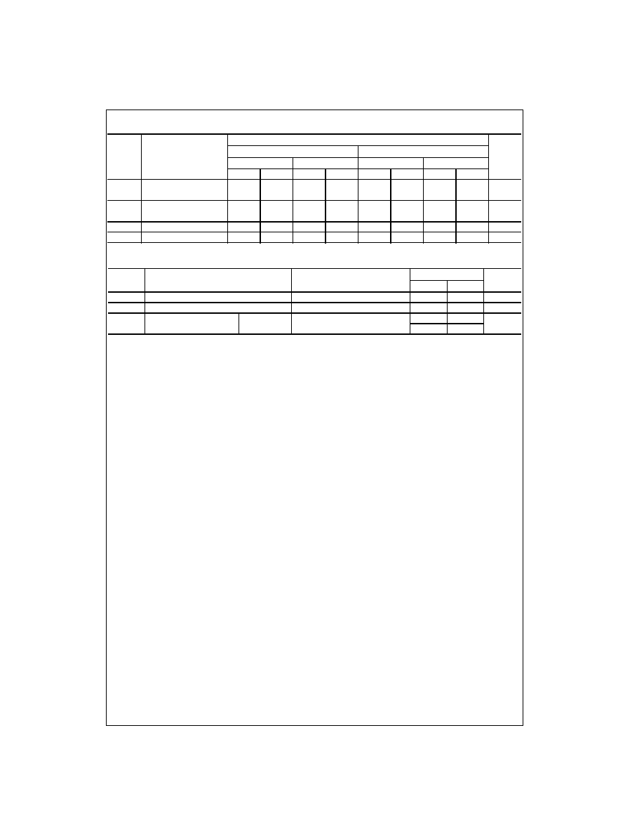
AC Electrical Characteristics
Capacitance
Symbol
Parameter
T
A
40
q
C to
85
q
C, R
L
500
:
Units
C
L
50 pF
C
L
30 pF
V
CC
3.3V
r
0.3V
V
CC
2.7V
V
CC
2.5V
r
0.2V
V
CC
1.8V
r
0.15V
Min
Max
Min
Max
Min
Max
Min
Max
t
PHL
, t
PLH
Propagation Delay
1.3
3.5
1.5
3.9
1.0
3.4
1.5
6.8
ns
Bus to Bus
t
PHL
, t
PLH
Propagation Delay
1.3
3.5
1.5
4.4
1.0
3.9
1.5
7.8
ns
LE to Bus
t
PZL
, t
PZH
Output Enable Time
1.3
4.0
1.5
5.1
1.0
4.6
1.5
9.2
ns
t
PLZ
, t
PHZ
Output Disable Time
1.3
4.0
1.5
4.3
1.0
3.8
1.5
6.8
ns
Symbol
Parameter
Conditions
T
A
25
q
C
Units
V
CC
Typical
C
IN
Input Capacitance
V
I
0V or V
CC
3.3
6
pF
C
OUT
Output Capacitance
V
I
0V or V
CC
3.3
7
pF
C
PD
Power Dissipation Capacitance Outputs Enabled f
10 MHz, C
L
50 pF
3.3
20
pF
2.5
20