© 2005 Fairchild Semiconductor Corporation
DS500692
www.fairchildsemi.com
October 2001
Revised May 2005
7
4
AL
VC1637
4
Low V
o
l
t
age 16-
B
i
t D-T
ype
Fl
ip-
F
lop
wit
h
3
.
6V T
o
ler
ant Inp
u
t
s
and Outpu
t
s
74ALVC16374
Low Voltage 16-Bit D-Type Flip-Flop
with 3.6V Tolerant Inputs and Outputs
General Description
The ALVC16374 contains sixteen non-inverting D-type flip-
flops with 3-STATE outputs and is intended for bus oriented
applications. The device is byte controlled. A buffered clock
(CP) and output enable (OE) are common to each byte and
can be shorted together for full 16-bit operation.
The 74ALVC16374 is designed for low voltage (1.65V to
3.6V) V
CC
applications with I/O compatibility up to 3.6V.
The 74ALVC16374 is fabricated with an advanced CMOS
technology to achieve high speed operation while maintain-
ing low CMOS power dissipation.
Features
s
1.65V - 3.6V V
CC
supply operation
s
3.6V tolerant inputs and outputs
s
t
PD
3.5 ns max for 3.0V to 3.6V V
CC
4.4 ns max for 2.3V to 2.7V V
CC
7.8 ns max for 1.65V to 1.95V V
CC
s
Power-off high impedance inputs and outputs
s
Supports live insertion and withdrawal (Note 1)
s
Uses patented noise/EMI reduction circuitry
s
Latchup conforms to JEDEC JED78
s
ESD performance:
Human body model
!
2000V
Machine model
!
200V
s
Also packaged in plastic Fine-Pitch Ball Grid Array
(FBGA)
Note 1: To ensure the high-impedance state during power up or power
down, OE should be tied to V
CC
through a pull-up resistor; the minimum
value of the resistor is determined by the current-sourcing capability of the
driver.
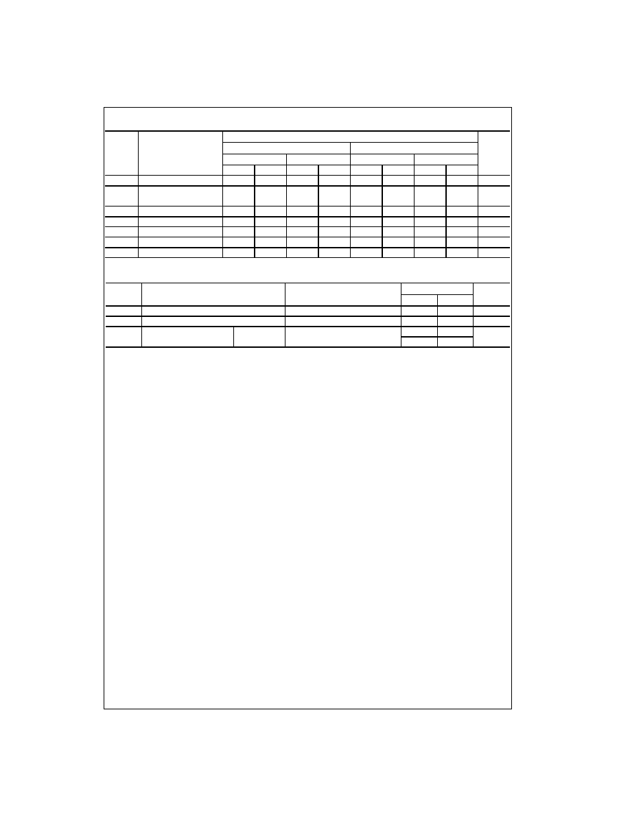
Ordering Code:
Note 2: BGA package available in Tape and Reel only.
Note 3: Devices also available in Tape and Reel. Specify by appending suffix letter "X" to the ordering code.
Order Number
Package Number
Package Descriptions
74ALVC16374GX
(Note 2)
BGA54A
54-Ball Fine-Pitch Ball Grid Array (FBGA), JEDEC MO-205, 5.5mm Wide
[TAPE and REEL]
74ALVC16374MTD
(Note 3)
MTD48
48-Lead Thin Shrink Small Outline Package (TSSOP), JEDEC MO-153, 6.1mm Wide

3
www.fairchildsemi.com
7
4
AL
VC1637
4
Functional Description
The 74ALVC16374 consists of sixteen edge-triggered
flip-flops with individual D-type inputs and 3-STATE true
outputs. The device is byte controlled with each byte func-
tioning identically, but independent of the other. The control
pins can be shorted together to obtain full 16-bit operation.
Each clock has a buffered clock and buffered Output
Enable common to all flip-flops within that byte. The
description which follows applies to each byte. Each
flip-flop will store the state of their individual I inputs that
meet the setup and hold time requirements on the
LOW-to-HIGH Clock (CP
n
) transition. With the Output
Enable (OE
n
) LOW, the contents of the flip-flops are avail-
able at the outputs. When OE
n
is HIGH, the outputs go to
the high impedance state. Operations of the OE
n
input
does not affect the state of the flip-flops.
Logic Diagram
Byte 1 (0:7)
Byte 2 (8:15)
Please note that this diagram is provided only for the understanding of logic operations and should not be used to estimate propagation delays.
www.fairchildsemi.com
4
74
A
L
VC16374
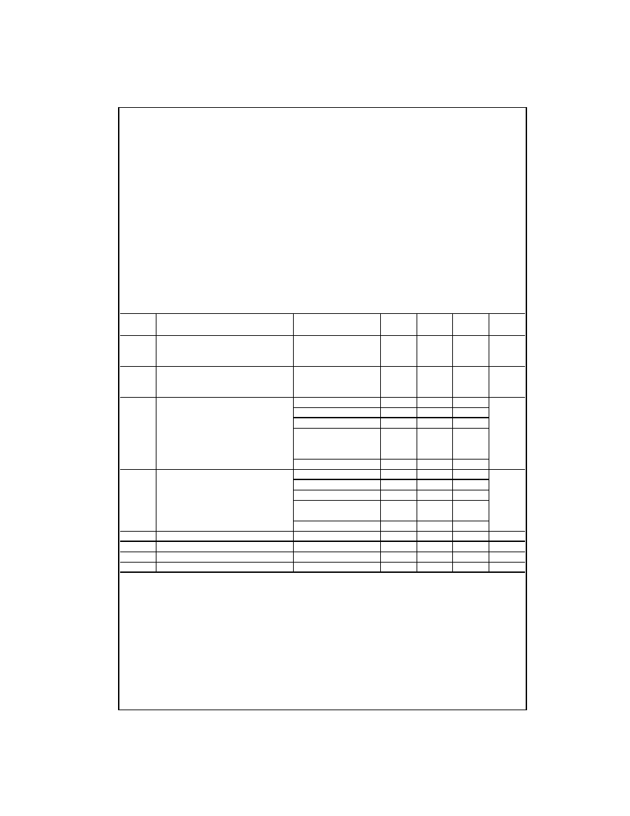
Absolute Maximum Ratings
(Note 4)
Recommended Operating
Conditions
(Note 6)
Note 4: The Absolute Maximum Ratings are those values beyond which
the safety of the device cannot be guaranteed. The device should not be
operated at these limits. The parametric values defined in the Electrical
Characteristics tables are not guaranteed at the Absolute Maximum Rat-
ings. The "Recommended Operating Conditions" table will define the condi-
tions for actual device operation.
Note 5: I
O
Absolute Maximum Rating must be observed.
Note 6: Floating or unused inputs must be held HIGH or LOW.
DC Electrical Characteristics
Supply Voltage (V
CC
)
0.5V to
4.6V
DC Input Voltage (V
I
)
0.5V to 4.6V
Output Voltage (V
O
) (Note 5)
0.5V to V
CC
0.5V
DC Input Diode Current (I
IK
)
V
I
0V
50 mA
DC Output Diode Current (I
OK
)
V
O
0V
50 mA
DC Output Source/Sink Current
(I
OH
/I
OL
)
r
50 mA
DC V
CC
or GND Current per
Supply Pin (I
CC
or GND)
r
100 mA
Storage Temperature Range (T
STG
)
65
q
C to
150
q
C
Power Supply
Operating 1.65V
to
3.6V
Input Voltage (V
I
)
0V to V
CC
Output Voltage (V
O
)
0V to V
CC
Free Air Operating Temperature (T
A
)
40
q
C to
85
q
C
Minimum Input Edge Rate (
'
t/
'
V)
V
IN
0.8V to 2.0V, V
CC
3.0V
10 ns/V
Symbol
Parameter
Conditions
V
CC
Min
Max
Units
(V)
V
IH
HIGH Level Input Voltage
1.65 -1.95
0.65 x V
CC
V
2.3 - 2.7
1.7
2.7 - 3.6
2.0
V
IL
LOW Level Input Voltage
1.65 -1.95
0.35 x V
CC
V
2.3 - 2.7
0.7
2.7 - 3.6
0.8
V
OH
HIGH Level Output Voltage
I
OH
100
P
A
1.65 - 3.6
V
CC
- 0.2
V
I
OH
4 mA
1.65
1.2
I
OH
6 mA
2.3
2
I
OH
12 mA
2.3
1.7
2.7
2.2
3.0
2.4
I
OH
24 mA
3.0
2
V
OL
LOW Level Output Voltage
I
OL
100
P
A
1.65 - 3.6
0.2
V
I
OL
4 mA
1.65
0.45
I
OL
6 mA
2.3
0.4
I
OL
12mA
2.3
0.7
2.7
0.4
I
OL
24 mA
3
0.55
I
I
Input Leakage Current
0
d
V
I
d
3.6V
3.6
r
5.0
P
A
I
OZ
3-STATE Output Leakage
0
d
V
O
d
3.6V
3.6
r
10
P
A
I
CC
Quiescent Supply Current
V
I
V
CC
or GND, I
O
0
3.6
40
P
A
'
I
CC
Increase in I
CC
per Input
V
IH
V
CC
0.6V
3 -3.6
750
P
A