© 2001 Fairchild Semiconductor Corporation
DS500682
www.fairchildsemi.com
October 2001
Revised October 2001
7
4
AL
VC1660
1
Low V
o
l
t
a
g
e
18-
Bit
Uni
ver
sal Bus
T
r
anscei
vers
wit
h
3.6V T
o
ler
a
nt Inp
u
ts and O
u
t
puts
74ALVC16601
Low Voltage 18-Bit Universal Bus Transceivers
with 3.6V Tolerant Inputs and Outputs
General Description
The ALVC16601 is an 18-bit universal bus transceiver
which combines D-type latches and D-type flip-flops to
allow data flow in transparent, latched, and clocked modes.
Data flow in each direction is controlled by output-enable
(OEAB and OEBA), latch-enable (LEAB and LEBA), and
clock (CLKAB and CLKBA) inputs. The clock can be con-
trolled by the clock-enable (CLKENAB and CLKENBA)
inputs. For A-to-B data flow, the device operates in the
transparent mode when LEAB is HIGH. When LEAB is
LOW, the A data is latched if CLKAB is held at a HIGH-to-
LOW logic level. If LEAB is LOW, the A bus data is stored
in the latch/flip-flop on the LOW-to-HIGH transition of
CLKAB. When OEAB is LOW, the outputs are active. When
OEAB is HIGH, the outputs are in the high-impedance
state.
Data flow for B to A is similar to that of A to B but uses
OEBA, LEBA, CLKBA and CLKENBA.
The ALVC16601 is designed for low voltage (1.65V to
3.6V) V
CC
applications with I/O capability up to 3.6V.
The ALVC16601 is fabricated with an advanced CMOS
technology to achieve high speed operation while maintain-
ing low CMOS power dissipation.
Features
s
1.65V≠3.6V V
CC
supply operation
s
3.6V tolerant inputs and outputs
s
t
PD
(A to B, B to A)
3.4 ns max for 3.0V to 3.6V V
CC
4.0 ns max for 2.3V to 2.7V V
CC
7.0 ns max for 1.65V 1.95V V
CC
s
Power-down high impedance inputs and outputs
s
Supports live insertion/withdrawal (Note 1)
s
Uses patented noise/EMI reduction circuitry
s
Latchup conforms to JEDEC JED78
s
ESD performance:
Human body model
>
2000V
Machine model
>
200V
s
Also packaged in plastic Fine-Pitch Ball Grid Array
(FBGA) (Preliminary)
Note 1: To ensure the high-impedance state during power up or power
down, OE should be tied to V
CC
through a pull-up resistor; the minimum
value of the resistor is determined by the current-sourcing capability of the
driver.
Ordering Code:
Note 2: BGA package available in Tape and Reel only.
Note 3: Devices also available in Tape and Reel. Specify by appending the suffix letter "X" to the ordering code.
Order Number
Package Number
Package Description
74ALVC16601GX
(Note 2)
BGA54A
(Preliminary)
54-Ball Fine-Pitch Ball Grid Array (FBGA), JEDEC MO-205, 5.5mm Wide
[TAPE and REEL]
74ALVC16601MTD
(Note 3)
MTD56
56-Lead Thin Shrink Small Outline Package (TSSOP), JEDEC MO-153, 6.1mm Wide
www.fairchildsemi.com
2
74
A
L
VC16601
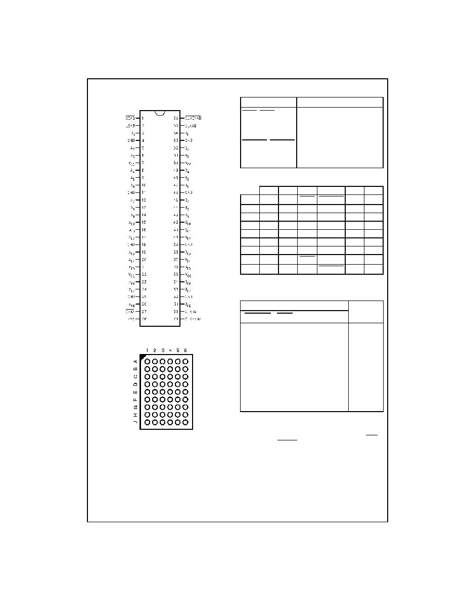
Connection Diagrams
Pin Assignment for TSSOP
Pin Assignment for FBGA
(Top Thru View)
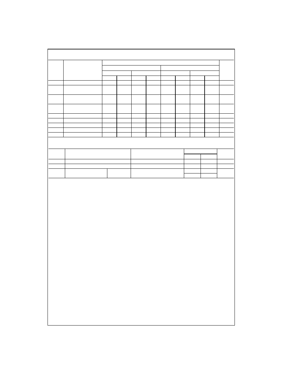
Pin Descriptions
FBGA Pin Assignments
Truth Table
(Note 4)
H
=
HIGH Voltage Level
L
=
LOW Voltage Level
X
=
Immaterial (HIGH or LOW, inputs may not float)
Z
=
High Impedance
Note 4: A-to-B data flow is shown; B-to-A flow is similar but uses OEBA,
LEBA, CLKBA, and CLKENBA.
Note 5: Output level before the indicated steady-state input conditions
were established.
Note 6: Output level before the indicated steady-state input conditions
were established, provided that CLKAB was HIGH before LEAB went LOW.
Pin Names
Description
OEAB, OEBA
Output Enable Inputs (Active LOW)
LEAB, LEBA
Latch Enable Inputs
CLKAB, CLKBA
Clock Inputs
CLKENAB, CLKENBA Clock Enable Inputs
A
1
≠A
18
Side A Inputs or 3-STATE Outputs
B
1
≠B
18
Side B Inputs or 3-STATE Outputs
1
2
3
4
5
6
A
A
2
A
1
OEAB CLKENAB
B
1
B
2
B
A
4
A
3
LEAB
CLKAB
B
3
B
4
C
A
6
A
5
V
CC
V
CC
B
5
B
6
D
A
8
A
7
GND
GND
B
7
B
8
E
A
10
A
9
GND
GND
B
9
B
10
F
A
12
A
11
GND
GND
B
11
B
12
G
A
14
A
13
V
CC
V
CC
B
13
B
14
H
A
16
A
15
OEBA
CLKBA
B
15
B
16
J
A
17
A
18
LEBA CLKENBA
B
18
B
17
Inputs
Outputs
CLKENAB
OEAB LEAB CLKAB
A
n
B
n
X
H
X
X
X
Z
X
L
H
X
L
L
X
L
H
X
H
H
H
L
L
X
X
B
0
(Note 5)
H
L
L
X
X
B
0
(Note 5)
L
L
L
L
L
L
L
L
H
H
L
L
L
L
X
B
0
(Note 5)
L
L
L
H
X
B
0
(Note 6)
3
www.fairchildsemi.com
7
4
AL
VC1660
1
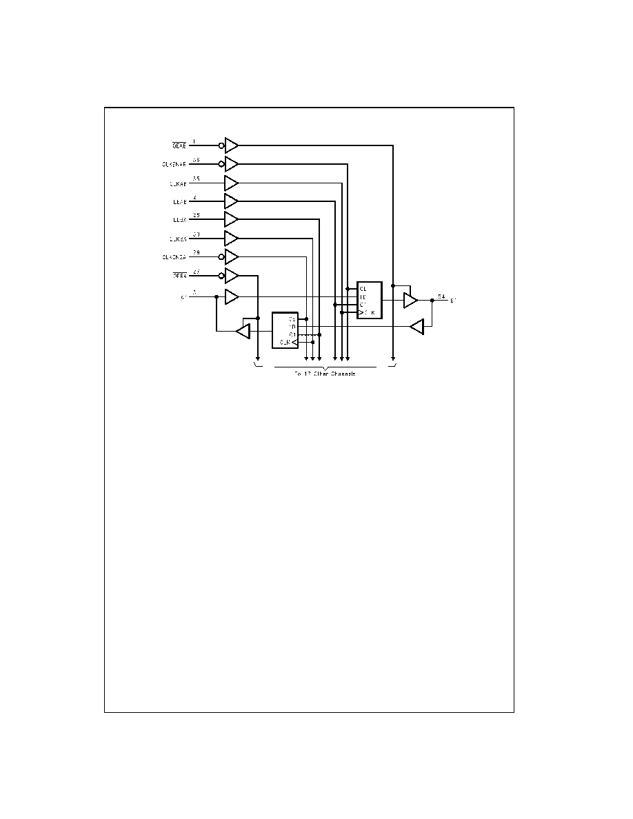
Logic Diagram
www.fairchildsemi.com
4
74
A
L
VC16601
Absolute Maximum Ratings
(Note 7)
Recommended Operating
Conditions
(Note 9)
Note 7: The Absolute Maximum Ratings are those values beyond which
the safety of the device cannot be guaranteed. The device should not be
operated at these limits. The parametric values defined in the Electrical
Characteristics tables are not guaranteed at the Absolute Maximum Rat-
ings. The "Recommended Operating Conditions" table will define the condi-
tions for actual device operation.
Note 8: I
O
Absolute Maximum Rating must be observed.
Note 9: Floating or unused inputs must be held HIGH or LOW.
DC Electrical Characteristics
Supply Voltage (V
CC
)
-
0.5V to
+
4.6V
DC Input Voltage (V
I
)
-
0.5V to 4.6V
Output Voltage (V
O
) (Note 8)
-
0.5V to V
CC
+
0.5V
DC Input Diode Current (I
IK
)
V
I
<
0V
-
50 mA
DC Output Diode Current (I
OK
)
V
O
<
0V
-
50 mA
DC Output Source/Sink Current
(I
OH
/I
OL
)
±
50 mA
DC V
CC
or GND Current per
Supply Pin (I
CC
or GND)
±
100 mA
Storage Temperature Range (T
STG
)
-
65
∞
C to
+
150
∞
C
Power Supply
Operating 1.65V
to
3.6V
Input Voltage (V
I
)
0V to V
CC
Output Voltage (V
O
)
0V to V
CC
Free Air Operating Temperature (T
A
)
-
40
∞
C to
+
85
∞
C
Minimum Input Edge Rate (
t/
V)
V
IN
=
0.8V to 2.0V, V
CC
=
3.0V
10 ns/V
Symbol
Parameter
Conditions
V
CC
Min
Max
Units
(V)
V
IH
HIGH Level Input Voltage
1.65 -1.95
0.65 x V
CC
V
2.3 - 2.7
1.7
2.7 - 3.6
2.0
V
IL
LOW Level Input Voltage
1.65 -1.95
0.35 x V
CC
V
2.3 - 2.7
0.7
2.7 - 3.6
0.8
V
OH
HIGH Level Output Voltage
I
OH
=
-
100
µ
A
1.65 - 3.6
V
CC
- 0.2
V
I
OH
=
-
4 mA
1.65
1.2
I
OH
=
-
6 mA
2.3
2
I
OH
=
-
12 mA
2.3
1.7
2.7
2.2
3.0
2.4
I
OH
=
-
24 mA
3.0
2
V
OL
LOW Level Output Voltage
I
OL
=
100
µ
A
1.65 - 3.6
0.2
V
I
OL
=
4 mA
1.65
0.45
I
OL
=
6 mA
2.3
0.4
I
OL
=
12mA
2.3
0.7
2.7
0.4
I
OL
=
24 mA
3
0.55
I
I
Input Leakage Current
0
V
I
3.6V
3.6
±
5.0
µ
A
I
OZ
3-STATE Output Leakage
0
V
O
3.6V
3.6
±
10
µ
A
I
CC
Quiescent Supply Current
V
I
=
V
CC
or GND, I
O
=
0
3.6
40
µ
A
I
CC
Increase in I
CC
per Input
V
IH
=
V
CC
-
0.6V
3 -3.6
750
µ
A
5
www.fairchildsemi.com
7
4
AL
VC1660
1
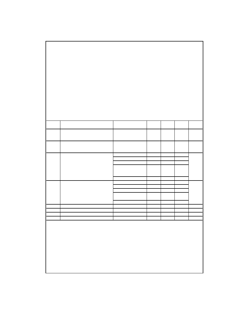
AC Electrical Characteristics
Capacitance
Symbol
Parameter
T
A
=
-
40
∞
C to
+
85
∞
C, R
L
=
500
Units
C
L
=
50 pF
C
L
=
30 pF
V
CC
=
3.3V
±
0.3V
V
CC
=
2.7V
V
CC
=
2.5V
±
0.2V
V
CC
=
1.8V
±
0.15V
Min
Max
Min
Max
Min
Max
Min
Max
f
MAX
Maximum Clock Frequency
250
200
200
100
ns
t
PHL
, t
PLH
Propagation Delay
1.3
3.4
1.5
4.0
1.0
3.5
1.5
7.0
ns
Bus to Bus
t
PHL
, t
PLH
Propagation Delay
1.3
4.0
1.5
4.9
1.0
4.4
1.5
8.8
ns
CLK to Bus
t
PHL
, t
PLH
Propagation Delay
1.3
4.0
1.5
4.9
1.0
4.4
1.5
8.8
ns
LE to Bus
t
PZL
, t
PZH
Output Enable Time
1.3
4.3
1.5
5.4
1.0
4.9
1.5
9.8
ns
t
PLZ
, t
PHZ
Output Disable Time
1.3
4.2
1.5
4.7
1.0
4.2
1.5
7.6
ns
t
W
Pulse Width
1.5
1.5
1.5
4.0
ns
t
S
Setup Time
1.5
1.5
1.5
2.5
ns
t
H
Hold Time
1.0
1.0
1.0
1.0
ns
Symbol
Parameter
Conditions
T
A
=
+
25
∞
C
Units
V
CC
Typical
C
IN
Input Capacitance
V
I
=
0V or V
CC
3.3
6
pF
C
OUT
Output Capacitance
V
I
=
0V or V
CC
3.3
7
pF
C
PD
Power Dissipation Capacitance Outputs Enabled f
=
10 MHz, C
L
=
50 pF
3.3
20
pF
2.5
20
www.fairchildsemi.com
6
74
A
L
VC16601
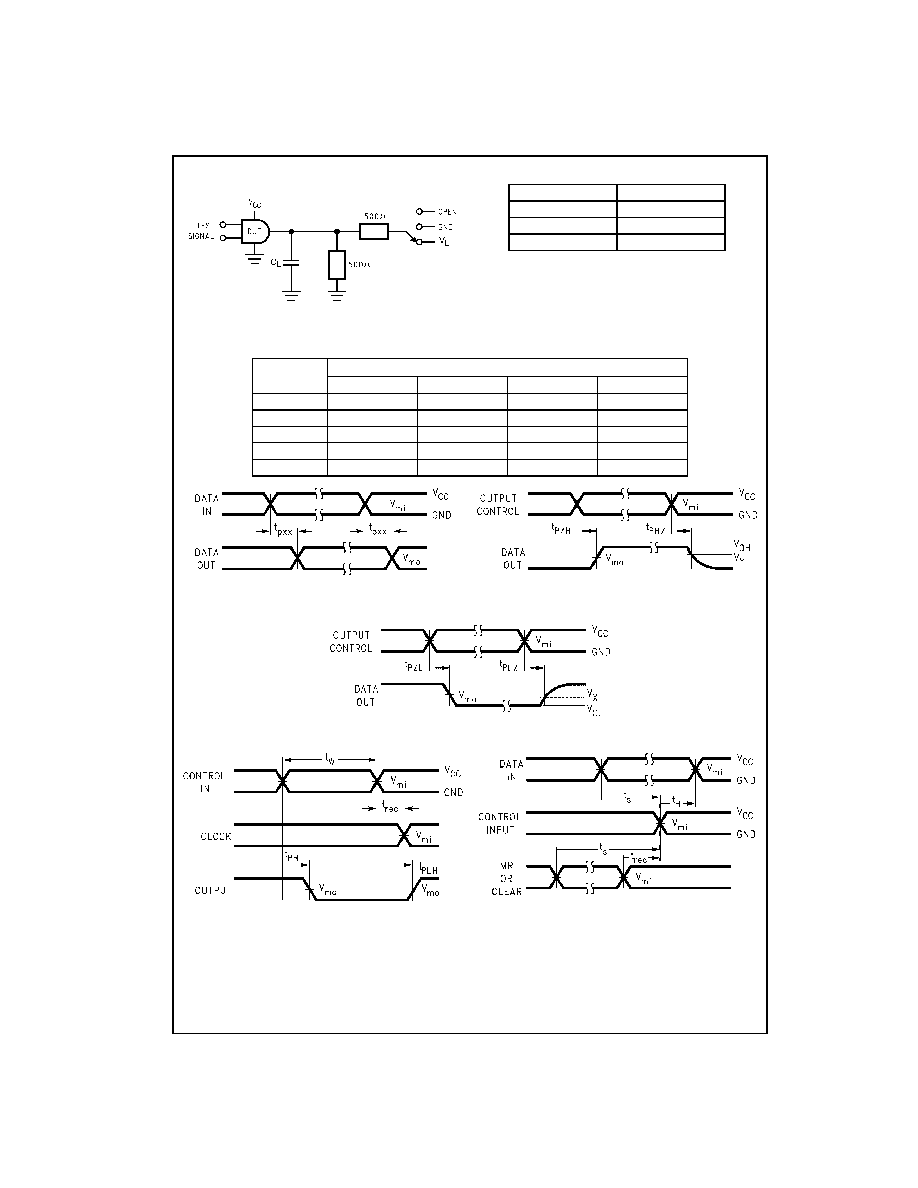
AC Loading and Waveforms
FIGURE 1. AC Test Circuit
TABLE 1. Values for Figure 1
TABLE 2. Variable Matrix
(Input Characteristics: f
=
1MHz; t
r
=
t
f
=
2ns; Z
0
=
50
FIGURE 2. Waveform for Inverting and
Non-inverting Functions
FIGURE 3. 3-STATE Output High Enable and
Disable Times for Low Voltage Logic
FIGURE 4. 3-STATE Output Low Enable and Disable Times for Low Voltage Logic
FIGURE 5. Propagation Delay, Pulse Width and
t
rec
Waveforms
FIGURE 6. Setup Time, Hold Time and Recovery Time
for Low Voltage Logic
TEST
SWITCH
t
PLH
, t
PHL
Open
t
PZL
, t
PLZ
V
L
t
PZH
, t
PHZ
GND
Symbol
V
CC
3.3V
±
0.3V
2.7V
2.5V
±
0.2V
1.8V
±
0.15V
V
mi
1.5V
1.5V
V
CC
/2
V
CC
/2
V
mo
1.5V
1.5V
V
CC
/2
V
CC
/2
V
X
V
OL
+
0.3V
V
OL
+
0.3V
V
OL
+
0.15V
V
OL
+
0.15V
V
Y
V
OH
-
0.3V
V
OH
-
0.3V
V
OH
-
0.15V
V
OH
-
0.15V
V
L
6V
6V
V
CC
*2
V
CC
*2
7
www.fairchildsemi.com
7
4
AL
VC1660
1
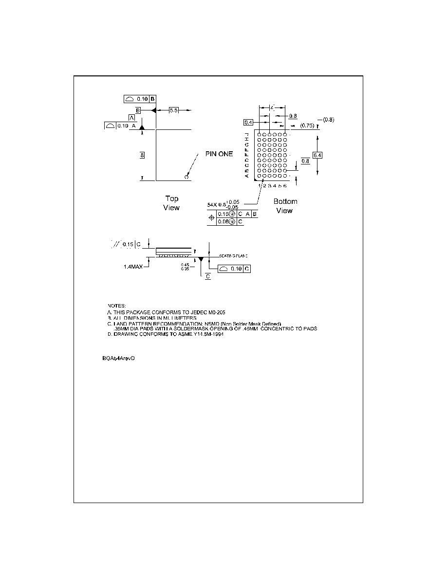
Physical Dimensions
inches (millimeters) unless otherwise noted
54-Ball Fine-Pitch Ball Grid Array (FBGA), JEDEC MO-205, 5.5mm Wide
Package Number BGA54A
(Preliminary)
www.fairchildsemi.com
8
7
4
AL
VC1660
1
Low V
o
l
t
a
ge
18-
Bit
Uni
ver
sal Bus
T
r
anscei
vers
wit
h
3.6V T
o
ler
ant Inp
u
ts and O
u
t
puts
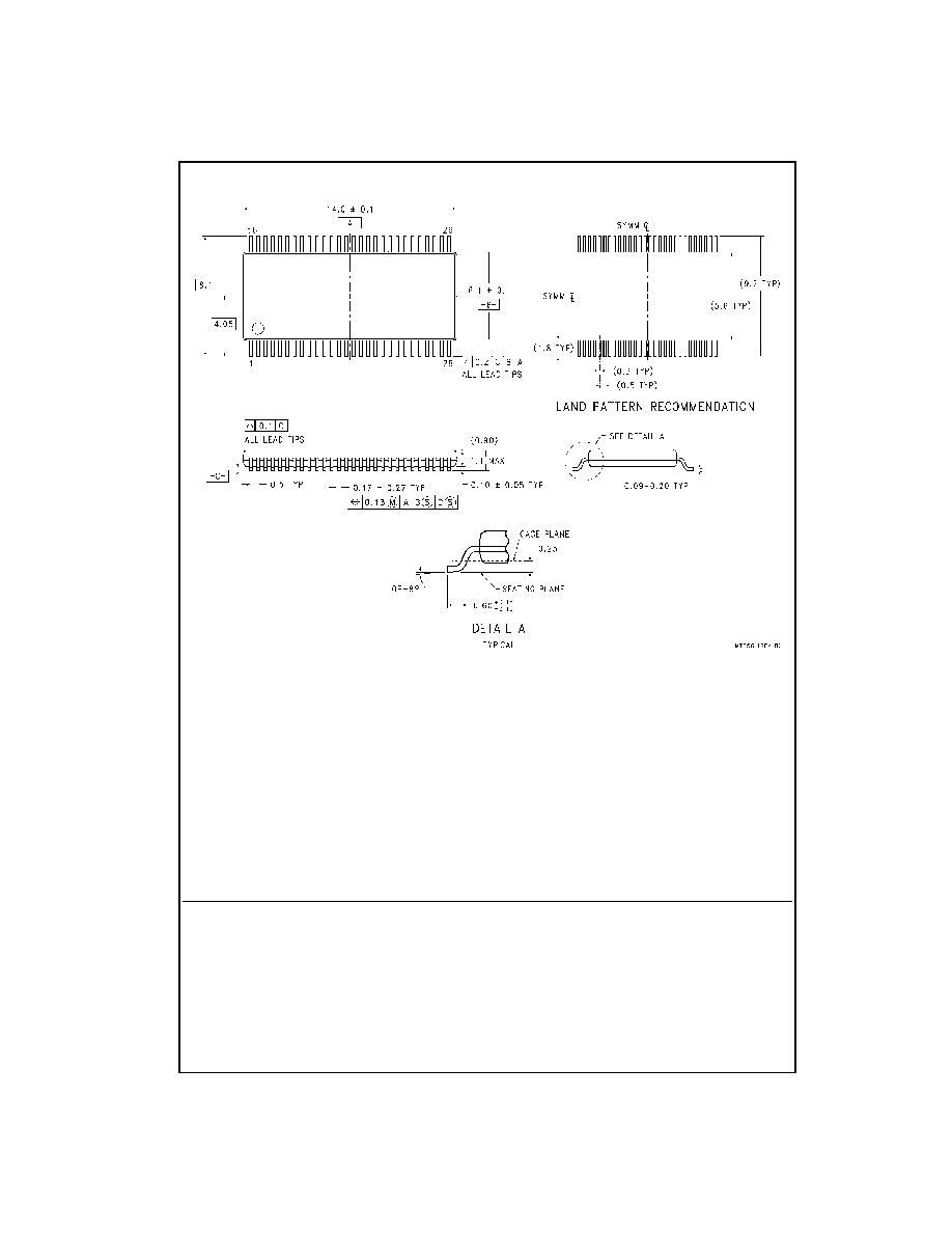
Physical Dimensions
inches (millimeters) unless otherwise noted (Continued)
56-Lead Thin Shrink Small Outline Package (TSSOP), JEDEC MO-153, 6.1mm Wide
Package Number MTD56
Fairchild does not assume any responsibility for use of any circuitry described, no circuit patent licenses are implied and
Fairchild reserves the right at any time without notice to change said circuitry and specifications.
LIFE SUPPORT POLICY
FAIRCHILD'S PRODUCTS ARE NOT AUTHORIZED FOR USE AS CRITICAL COMPONENTS IN LIFE SUPPORT
DEVICES OR SYSTEMS WITHOUT THE EXPRESS WRITTEN APPROVAL OF THE PRESIDENT OF FAIRCHILD
SEMICONDUCTOR CORPORATION. As used herein:
1. Life support devices or systems are devices or systems
which, (a) are intended for surgical implant into the
body, or (b) support or sustain life, and (c) whose failure
to perform when properly used in accordance with
instructions for use provided in the labeling, can be rea-
sonably expected to result in a significant injury to the
user.
2. A critical component in any component of a life support
device or system whose failure to perform can be rea-
sonably expected to cause the failure of the life support
device or system, or to affect its safety or effectiveness.
www.fairchildsemi.com