© 2002 Fairchild Semiconductor Corporation
ds500717
www.fairchildsemi.com
February 2002
Revised February 2002
7
4
AL
VC2245
Low
V
o
l
t
ag
e Bi
dir
ecti
onal
T
r
anscei
ver
wit
h
3.
6V T
o
l
e
rant
Input
s an
d Outp
uts
and
26
Seri
es
Res
i
st
ors in B
Out
puts
74ALVC2245
Low Voltage Bidirectional Transceiver
with 3.6V Tolerant Inputs and Outputs
and 26
Series Resistors in B Outputs
General Description
The ALVC2245 contains eight non-inverting bidirectional
buffers with 3-STATE outputs and is intended for bus ori-
ented applications. The T/R input determines the direction
of data flow. The OE input disables both the A and B ports
by placing them in a high impedance state.
The 74ALVC2245 is designed for low voltage (1.65V to
3.6V) V
CC
applications with I/O compatibility up to 3.6V.
The ALVC2245 is also designed with 26
series resistance
in the B Port outputs. This design reduces line noise in
applications such as memory address drivers, clock driv-
ers, and bus transceivers transmitters
The 74ALVC2245 is fabricated with an advanced CMOS
technology to achieve high-speed operation while main-
taining low CMOS power dissipation.
Features
s
1.65V to 3.6V V
CC
supply operation
s
3.6V tolerant inputs and outputs
s
26
series resistors in B Port outputs
s
Power-off high impedance inputs and outputs
s
Supports Live Insertion and Withdrawal (Note 1)
s
t
PD
(A to B)
4.9 ns max for 3.0V to 3.6V V
CC
6.1 ns max for 2.3V to 2.7V V
CC
9.8 ns max for 1.65V to 1.95V V
CC
s
Uses patented Quiet Series
noise/EMI reduction
circuitry
s
Latchup conforms to JEDEC JED78
s
ESD performance:
Human body model
>
2000V
Machine model
>
200V
Note 1: To ensure the high impedance state during power up and power
down, OE
n
should be tied to V
CC
through a pull up resistor. The minimum
value of the resistor is determined by the current sourcing capability of the
driver.
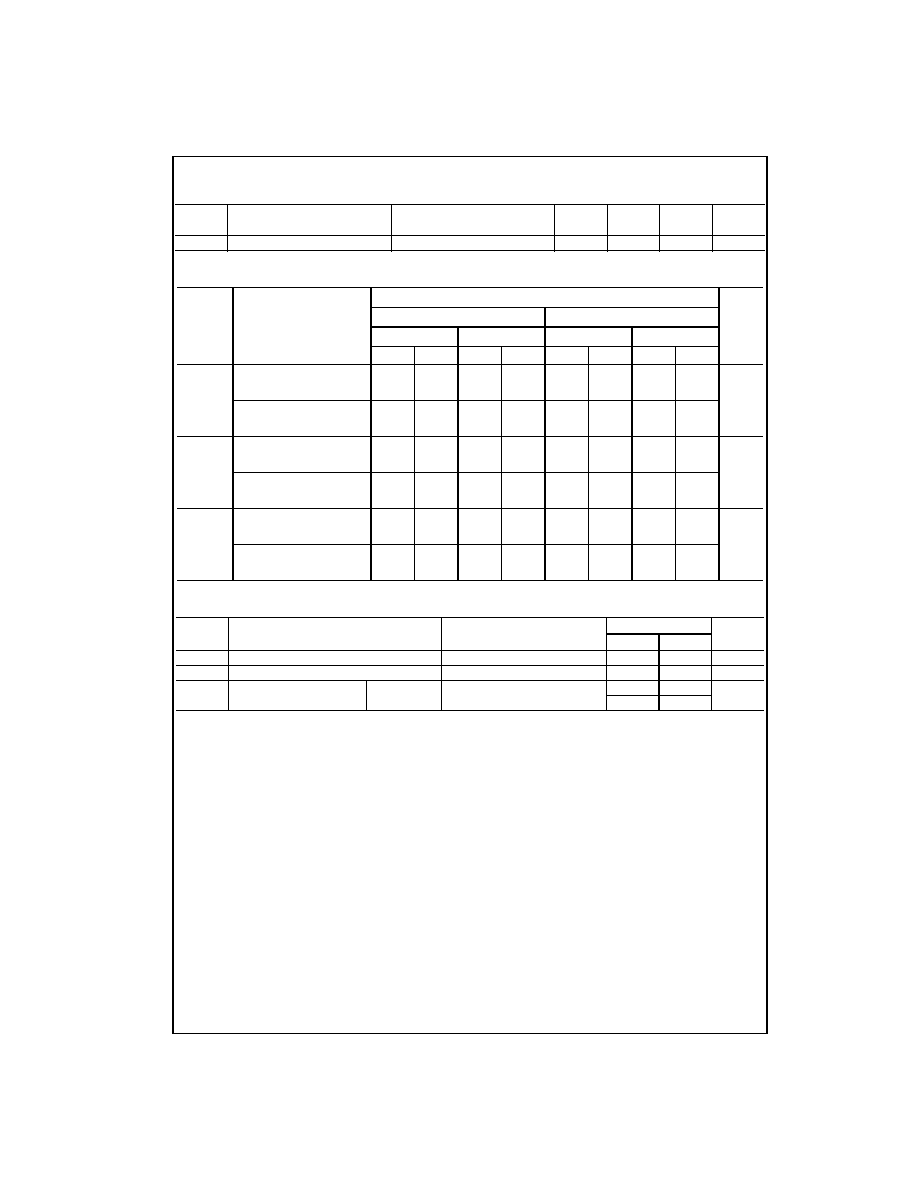
Ordering Code:
Devices also available in Tape and Reel. Specify by appending the suffix letter "X" to the ordering code.
Logic Symbol
Pin Descriptions
Quiet Series
is a trademark of Fairchild Semiconductor Corporation.
Order Number
Package Number
Package Description
74ALVC2245WM
M20B
20-Lead Small Outline Integrated Circuit (SOIC), JEDEC MS-013, 0.300" Wide
74ALVC2245MTC
MTC20
20-Lead Thin Shrink Small Outline Package (TSSOP), JEDEC MO-153, 4.4mm Wide
Pin Names
Description
OE
Output Enable Input (Active LOW)
T/R
Transmit/Receive Input
A
0
≠A
7
Side A Inputs or 3-STATE Outputs
B
0
≠B
7
Side B Inputs or 3-STATE Outputs
3
www.fairchildsemi.com
7
4
AL
VC2245
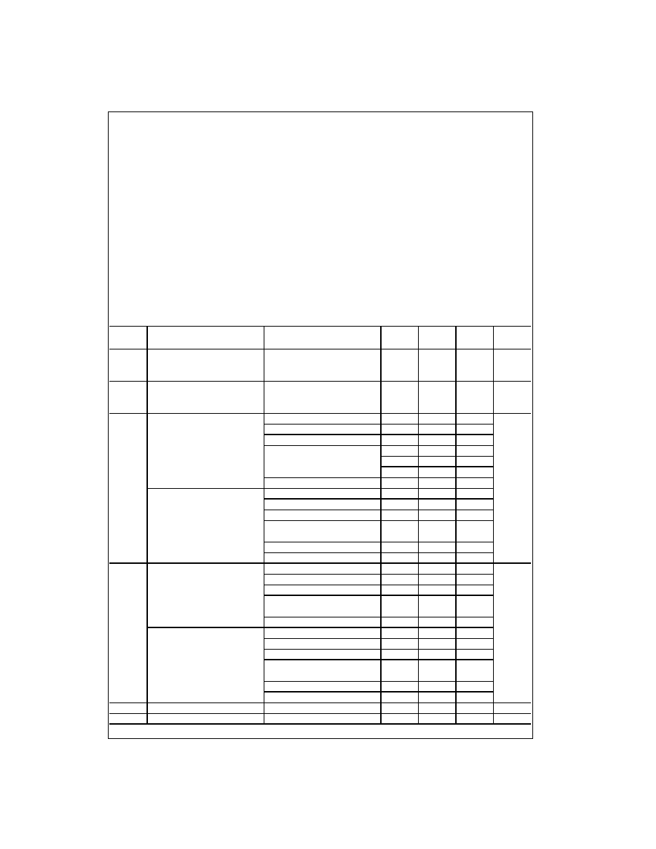
Absolute Maximum Ratings
(Note 3)
Recommended Operating
Conditions
(Note 5)
Note 3: The Absolute Maximum Ratings are those values beyond which
the safety of the device cannot be guaranteed. The device should not be
operated at these limits. The parametric values defined in the Electrical
Characteristics tables are not guaranteed at the Absolute Maximum Rat-
ings. The "Recommended Operating Conditions" table will define the condi-
tions for actual device operation.
Note 4: I
O
Absolute Maximum Rating must be observed.
Note 5: Floating or unused control inputs must be held HIGH or LOW.
DC Electrical Characteristics
Supply Voltage (V
CC
)
-
0.5V to
+
4.6V
DC Input Voltage (V
I
)
-
0.5V to 4.6V
Output Voltage (V
O
) (Note 4)
-
0.5V to V
CC
+
0.5V
DC Input Diode Current (I
IK
)
V
I
<
0V
-
50 mA
DC Output Diode Current (I
OK
)
V
O
<
0V
-
50 mA
DC Output Source/Sink Current
(I
OH
/I
OL
)
±
50 mA
DC V
CC
or GND Current per
Supply Pin (I
CC
or GND)
±
100 mA
Storage Temperature Range (T
STG
)
-
65
∞
C to
+
150
∞
C
Power Supply
Operating
1.65V to 3.6V
Input Voltage
0V to V
CC
Output Voltage (V
O
)
0V to V
CC
Free Air Operating Temperature (T
A
)
-
40
∞
C to
+
85
∞
C
Minimum Input Edge Rate (
t/
V)
V
IN
=
0.8V to 2.0V, V
CC
=
3.0V
10 ns/V
Symbol
Parameter
Conditions
V
CC
Min
Max
Units
(V)
V
IH
HIGH Level Input Voltage
1.65 - 1.95
0.65 x V
CC
V
2.3 - 2.7
1.7
2.7 - 3.6
2.0
V
IL
LOW Level Input Voltage
1.65 - 1.95
0.35 x V
CC
V
2.3 - 2.7
0.7
2.7 - 3.6
0.8
V
OH
HIGH Level Output Voltage
I
OH
=
-
100
µ
A
1.65 - 3.6
V
CC
- 0.2
V
A Outputs
I
OH
=
-
4 mA
1.65
1.2
I
OH
=
-
6 mA
2.3
2.0
I
OH
=
-
12 mA
2.3
1.7
2.7
2.2
3.0
2.4
I
OH
=
-
24 mA
3.0
2
HIGH Level Output Voltage
I
OH
=
-
100
µ
A
1.65 - 3.6
V
CC
- 0.2
B Outputs
I
OH
=
-
2 mA
1.65
1.2
I
OH
=
-
4 mA
2.3
1.9
I
OH
=
-
6 mA
2.3
1.7
3.0
2.4
I
OH
=
-
8 mA
2.7
2
I
OH
=
-
12 mA
3.0
2
V
OL
LOW Level Output Voltage
I
OL
=
100
µ
A
1.65 - 3.6
0.2
V
A Outputs
I
OL
=
4 mA
1.65
0.45
I
OL
=
6 mA
2.3
0.4
I
OL
=
12 mA
2.3
0.7
2.7
0.4
I
OL
=
24 mA
3.0
0.55
LOW Level Output Voltage
I
OL
=
100
µ
A
1.65 - 3.6
0.2
B Outputs
I
OL
=
2 mA
1.65
0.45
I
OL
=
4 mA
2.3
0.4
I
OL
=
6 mA
2.3
0.55
3.0
0.55
I
OL
=
8 mA
2.7
0.6
I
OL
=
12 mA
3.0
0.8
I
I
Input Leakage Current
0
V
I
3.6V
1.65 - 3.6
±
5.0
µ
A
I
CC
Quiescent Supply Current
V
I
=
V
CC
or GND, I
O
=
0
3.6
40
µ
A
5
www.fairchildsemi.com
7
4
AL
VC2245
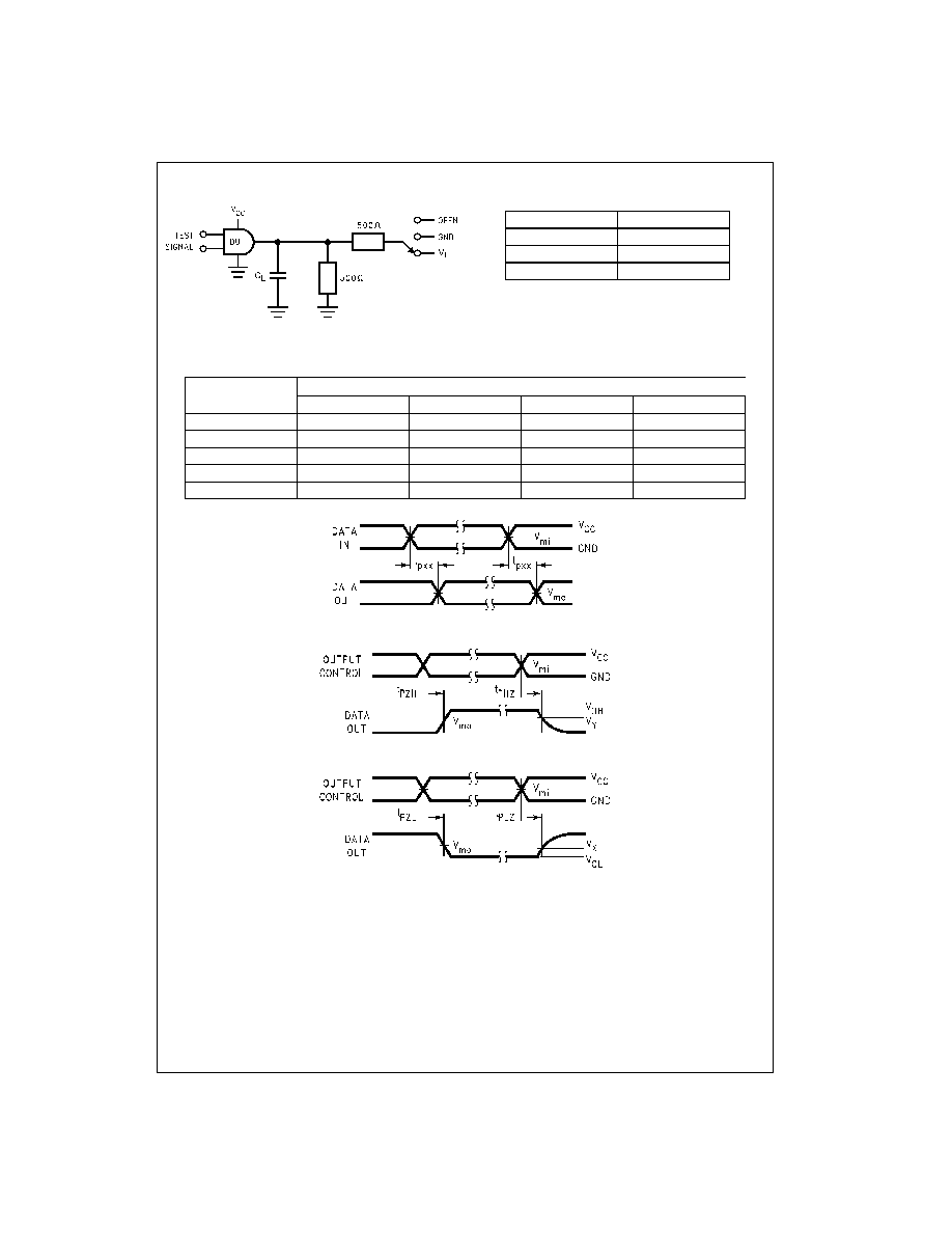
AC Loading and Waveforms
FIGURE 1. AC Test Circuit
TABLE 1. Values for Figure 1
TABLE 2. Variable Matrix
(Input Characteristics: f
=
1MHz; t
r
=
t
f
=
2ns; Z
O
=
50
)
FIGURE 2. Waveform for Inverting and Non-inverting Functions
FIGURE 3. 3-STATE Output High Enable and Disable Times for Low Voltage Logic
FIGURE 4. 3-STATE Output Low Enable and Disable Times for Low Voltage Logic
TEST
SWITCH
t
PLH
, t
PHL
Open
t
PZL
, t
PLZ
V
L
t
PZH
, t
PHZ
GND
Symbol
V
CC
3.3V
±
0.3V
2.7V
2.5
±
0.2V
1.8V
±
0.15V
V
mi
1.5V
1.5V
V
CC
/2
V
CC
/2
V
mo
1.5V
1.5V
V
CC
/2
V
CC
/2
V
X
V
OL
+
0.3V
V
OL
+
0.3V
V
OL
+
0.15V
V
OL
+
0.15V
V
Y
V
OH
-
0.3V
V
OH
-
0.3V
V
OH
-
0.15V
V
OH
-
0.15V
V
L
6V
6V
V
CC
*2
V
CC
*2