 | –≠–ª–µ–∫—Ç—Ä–æ–Ω–Ω—ã–π –∫–æ–º–ø–æ–Ω–µ–Ω—Ç: 74ALVC86 | –°–∫–∞—á–∞—Ç—å:  PDF PDF  ZIP ZIP |
© 2001 Fairchild Semiconductor Corporation
ds500718
www.fairchildsemi.com
December 2001
Revised December 2001
7
4
AL
VC86 Low
V
o
l
t
age Quad 2-I
nput Excl
usive-
OR
Gat
e
wi
th 3.6V T
o
ler
a
nt I
nputs and O
u
t
put
s
74ALVC86
Low Voltage Quad 2-Input Exclusive-OR Gate with
3.6V Tolerant Inputs and Outputs
General Description
The ALVC86 contains four 2-input exclusive OR gates.
This product is designed for low voltage (1.65V to 3.6V)
V
CC
applications with I/O compatibility up to 3.6V
The 74ALVC86 is fabricated with an advanced CMOS
technology to achieve high-speed operation while main-
taining low CMOS power dissipation.
Features
s
1.65V to 3.6V V
CC
supply operation
s
3.6V tolerant inputs and outputs
s
t
PD
3.5 ns max for 3.0V to 3.6V V
CC
4.4 ns max for 2.3V to 2.7V V
CC
7.8 ns max for 1.65V to 1.95V V
CC
s
Power-off high impedance inputs and outputs
s
Uses patented Quiet Series
noise/EMI reduction
circuitry
s
Latchup conforms to JEDEC JED78
s
ESD performance:
Human body model
>
2000V
Machine model
>
250V
Ordering Code:
Devices also available in Tape and Reel. Specify by appending the suffix letter "X" to the ordering code.
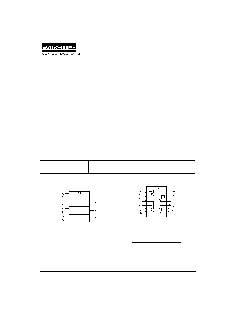
Logic Symbol
IEEE/IEC
Connection Diagram
Pin Descriptions
Quiet Series
is a trademark of Fairchild Semiconductor Corporation
Order Number
Package Number
Package Description
74ALVC86M
M14A
14-Lead Small Outline Integrated Circuit (SOIC), JEDEC MS-012, 0.150" Narrow
74ALVC86MTC
MTC14
14-Lead Thin Shrink Small Outline Package (TSSOP), JEDEC MO-153, 4.4mm Wide
Pin Names
Description
A
n
, B
n
Inputs
O
n
Outputs
www.fairchildsemi.com
2
74AL
V
C86
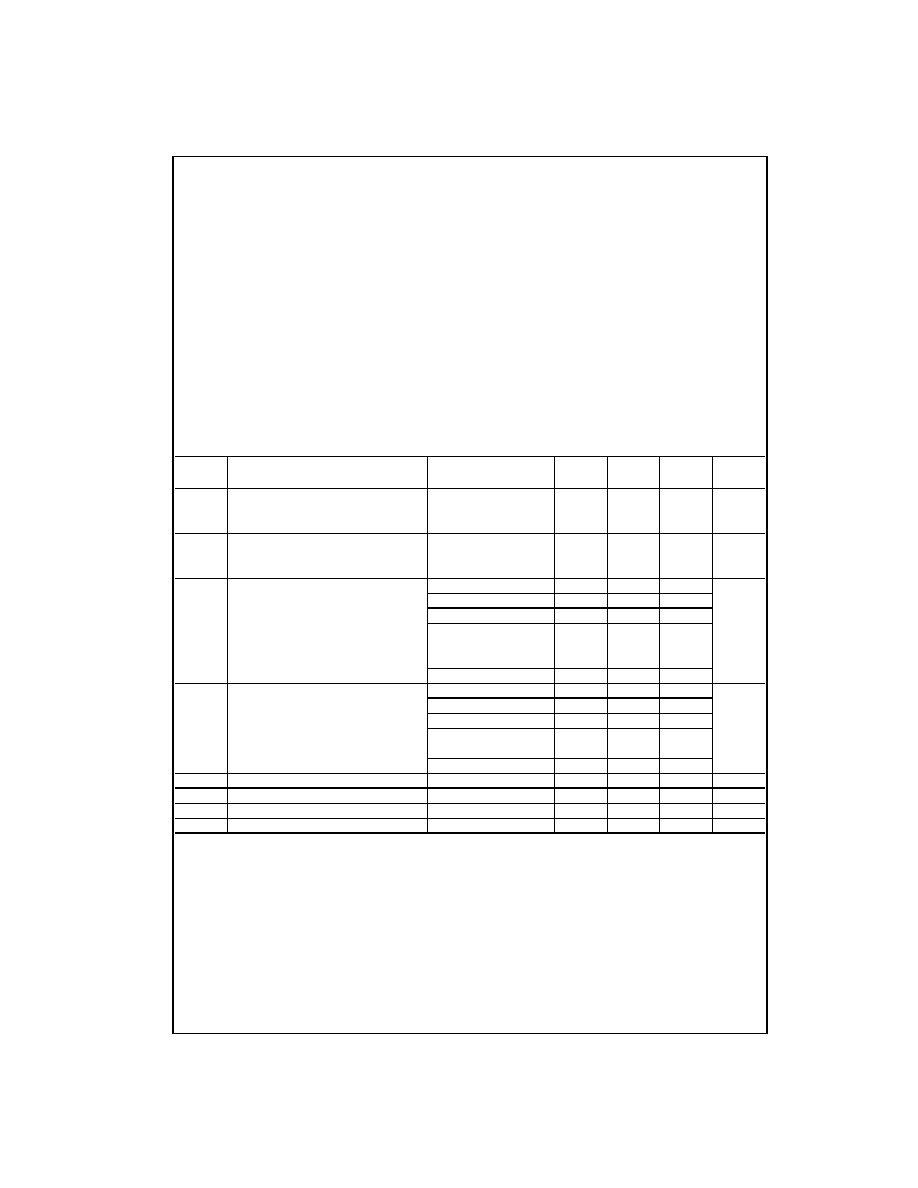
Absolute Maximum Ratings
(Note 1)
Recommended Operating
Conditions
(Note 3)
Note 1: The Absolute Maximum Ratings are those values beyond which
the safety of the device cannot be guaranteed. The device should not be
operated at these limits. The parametric values defined in the Electrical
Characteristics tables are not guaranteed at the Absolute Maximum Rat-
ings. The "Recommended Operating Conditions" table will define the condi-
tions for actual device operation.
Note 2: I
O
Absolute Maximum Rating must be observed.
Note 3: Floating or unused inputs must be held HIGH or LOW.
DC Electrical Characteristics
Supply Voltage (V
CC
)
-
0.5V to
+
4.6V
DC Input Voltage (V
I
)
-
0.5V to 4.6V
Output Voltage (V
O
) (Note 2)
-
0.5V to V
CC
+
0.5V
DC Input Diode Current (I
IK
)
V
I
<
0V
-
50 mA
DC Output Diode Current (I
OK
)
V
O
<
0V
-
50 mA
DC Output Source/Sink Current
(I
OH
/I
OL
)
±
50 mA
DC V
CC
or GND Current per
Supply Pin (I
CC
or GND)
±
100 mA
Storage Temperature Range (T
STG
)
-
65
∞
C to
+
150
∞
C
Power Supply
Operating 1.65V
to
3.6V
Input Voltage (V
I
)
0V to V
CC
Output Voltage (V
O
)
0V to V
CC
Free Air Operating Temperature (T
A
)
-
40
∞
C to
+
85
∞
C
Minimum Input Edge Rate (
t/
V)
V
IN
=
0.8V to 2.0V, V
CC
=
3.0V
10 ns/V
Symbol
Parameter
Conditions
V
CC
Min
Max
Units
(V)
V
IH
HIGH Level Input Voltage
1.65 -1.95
0.65 x V
CC
V
2.3 - 2.7
1.7
2.7 - 3.6
2.0
V
IL
LOW Level Input Voltage
1.65 -1.95
0.35 x V
CC
V
2.3 - 2.7
0.7
2.7 - 3.6
0.8
V
OH
HIGH Level Output Voltage
I
OH
=
-
100
µ
A
1.65 - 3.6
V
CC
- 0.2
V
I
OH
=
-
4 mA
1.65
1.2
I
OH
=
-
6 mA
2.3
2
I
OH
=
-
12 mA
2.3
1.7
2.7
2.2
3.0
2.4
I
OH
=
-
24 mA
3.0
2
V
OL
LOW Level Output Voltage
I
OL
=
100
µ
A
1.65 - 3.6
0.2
V
I
OL
=
4 mA
1.65
0.45
I
OL
=
6 mA
2.3
0.4
I
OL
=
12mA
2.3
0.7
2.7
0.4
I
OL
=
24 mA
3
0.55
I
I
Input Leakage Current
0
V
I
3.6V
3.6
±
5.0
µ
A
I
OZ
3-STATE Output Leakage
0
V
O
3.6V
3.6
±
10
µ
A
I
CC
Quiescent Supply Current
V
I
=
V
CC
or GND, I
O
=
0
3.6
40
µ
A
I
CC
Increase in I
CC
per Input
V
IH
=
V
CC
-
0.6V
3 -3.6
750
µ
A
3
www.fairchildsemi.com
74
A
L
V
C
8
6
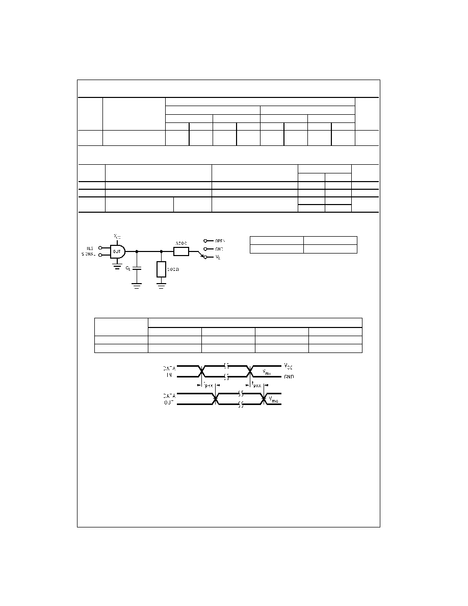
AC Electrical Characteristics
Capacitance
AC Loading and Waveforms
FIGURE 1. AC Test Circuit
TABLE 1. Values for Figure 1
TABLE 2. Variable Matrix
(Input Characteristics: f
=
1MHz; t
r
=
t
f
=
2ns; Z
0
=
50
FIGURE 2. Waveform for Inverting and Non-inverting Functions
Symbol
Parameter
T
A
=
-
40
∞
C to
+
85
∞
C, R
L
=
500
Units
C
L
=
50 pF
C
L
=
30 pF
V
CC
=
3.3V
±
0.3V
V
CC
=
2.7V
V
CC
=
2.5V
±
0.2V
V
CC
=
1.8V
±
0.15V
Min
Max
Min
Max
Min
Max
Min
Max
t
PHL
, t
PLH
Propagation Delay
1.1
3.5
1.3
4.4
0.8
3.9
1.0
7.8
ns
Bus to Bus
Symbol
Parameter
Conditions
T
A
=
+
25
∞
C
Units
V
CC
Typical
C
IN
Input Capacitance
V
I
=
0V or V
CC
3.3
6
pF
C
OUT
Output Capacitance
V
I
=
0V or V
CC
3.3
7
pF
C
PD
Power Dissipation Capacitance Outputs Enabled f
=
10 MHz, C
L
=
50 pF
3.3
20
pF
2.5
20
TEST
SWITCH
t
PLH
,t
PHL
Open
Symbol
V
CC
3.3V
±
0.3V
2.7V
2.5V
±
0.2V
1.8V
±
0.15V
V
mi
1.5V
1.5V
V
CC
/2
V
CC
/2
V
mo
1.5V
1.5V
V
CC
/2
V
CC
/2
www.fairchildsemi.com
4
74AL
V
C86
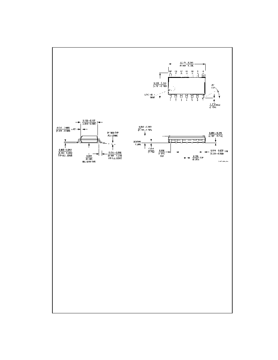
Physical Dimensions
inches (millimeters) unless otherwise noted
14-Lead Small Outline Integrated Circuit (SOIC), JEDEC MS-012, 0.150" Narrow
Package Number M14A
5
www.fairchildsemi.com
7
4
AL
VC86 Low
V
o
l
t
age Quad 2-I
nput Excl
usive-
OR
Gat
e
wi
th 3.6V T
o
ler
a
nt I
nputs and O
u
t
put
s
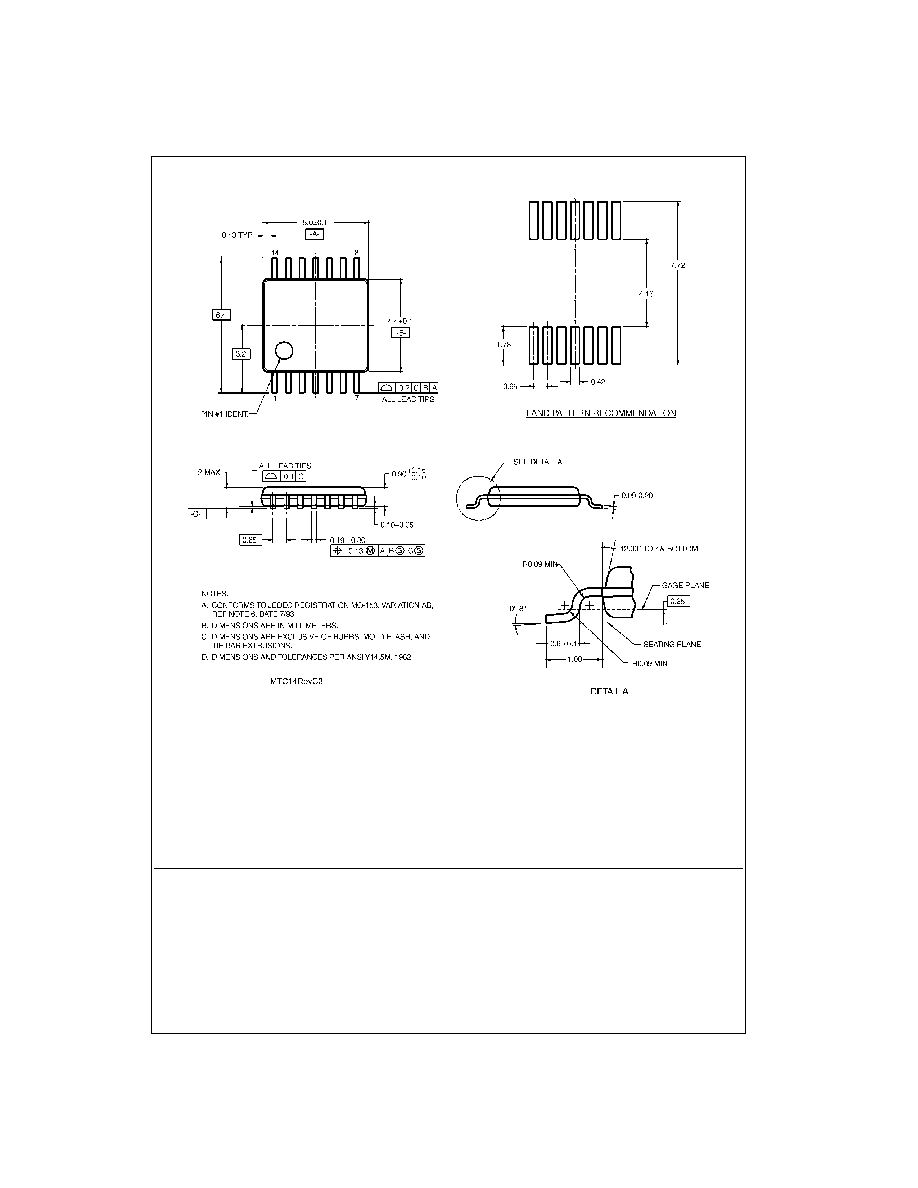
Physical Dimensions
inches (millimeters) unless otherwise noted (Continued)
14-Lead Thin Shrink Small Outline Package (TSSOP), JEDEC MO-153, 4.4mm Wide
Package Number MTC14
Fairchild does not assume any responsibility for use of any circuitry described, no circuit patent licenses are implied and
Fairchild reserves the right at any time without notice to change said circuitry and specifications.
LIFE SUPPORT POLICY
FAIRCHILD'S PRODUCTS ARE NOT AUTHORIZED FOR USE AS CRITICAL COMPONENTS IN LIFE SUPPORT
DEVICES OR SYSTEMS WITHOUT THE EXPRESS WRITTEN APPROVAL OF THE PRESIDENT OF FAIRCHILD
SEMICONDUCTOR CORPORATION. As used herein:
1. Life support devices or systems are devices or systems
which, (a) are intended for surgical implant into the
body, or (b) support or sustain life, and (c) whose failure
to perform when properly used in accordance with
instructions for use provided in the labeling, can be rea-
sonably expected to result in a significant injury to the
user.
2. A critical component in any component of a life support
device or system whose failure to perform can be rea-
sonably expected to cause the failure of the life support
device or system, or to affect its safety or effectiveness.
www.fairchildsemi.com