© 2001 Fairchild Semiconductor Corporation
DS500708
www.fairchildsemi.com
November 2001
Revised November 2001
7
4
AL
VCH16237
3 Low
V
o
l
t
a
g
e 16-
Bit
T
r
anspar
ent
Lat
c
h wi
th
Bushold
and
26
Ser
i
es
Resi
stor
s i
n
Out
puts
74ALVCH162373
Low Voltage 16-Bit Transparent Latch with Bushold
and 26
Series Resistors in Outputs
General Description
The ALVCH162373 contains sixteen non-inverting latches
with 3-STATE outputs and is intended for bus oriented
applications. The device is byte controlled. The flip-flops
appear to be transparent to the data when the Latch enable
(LE) is HIGH. When LE is LOW, the data that meets the
setup time is latched. Data appears on the bus when the
Output Enable (OE) is LOW. When OE is HIGH, the out-
puts are in a high impedance state.
The ALVCH162373 data inputs include active bushold cir-
cuitry, eliminating the need for external pull-up resistors to
hold unused or floating data inputs at a valid logic level.
The ALVCH162373 is also designed with 26
series resis-
tors in the outputs. This design reduces line noise in appli-
cations such as memory address driver, clock drivers and
bus transceivers/transmitters.
The 74ALVCH162373 is designed for low voltage (1.65V to
3.6V) V
CC
applications with output compatibility up to 3.6V.
The 74ALVCH162373 is fabricated with an advanced
CMOS technology to achieve high speed operation while
maintaining low CMOS power dissipation.
Features
s
1.65V to 3.6V V
CC
supply operation
s
3.6V tolerant control inputs and outputs
s
Bushold on data inputs eliminates the need for external
pull-up/pull-down resistors
s
26
series resistors in outputs
s
t
PD
(I
n
to O
n
)
3.8 ns max for 3.0V to 3.6V V
CC
5.0 ns max for 2.3V to 2.7V V
CC
9.0 ns max for 1.65V to 1.95V V
CC
s
Uses patented noise/EMI reduction circuitry
s
Latchup conforms to JEDEC JED78
s
ESD performance:
Human body model
>
2000V
Machine model
>
200V
Ordering Code:
Devices also available in Tape and Reel. Specify by appending the suffix letter "X" to the ordering code.
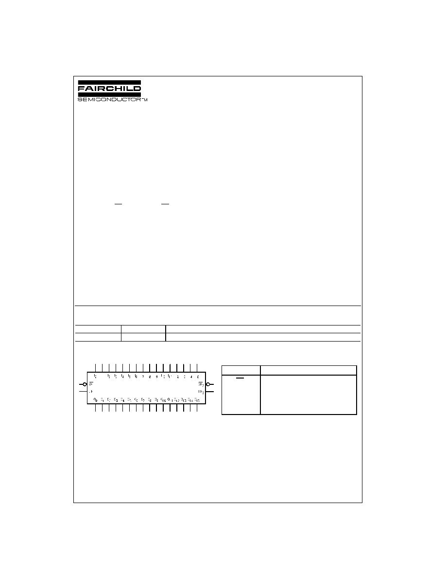
Logic Symbol
Pin Descriptions
Ordering Number Package Number
Package Description
74ALVCH162373T
MTD48
48-Lead Thin Shrink Small Outline Package (TSSOP), JEDEC MO-153, 6.1mm Wide
Pin Names
Description
OE
n
Output Enable Input (Active LOW)
LE
n
Latch Enable Input
I
0
≠I
15
Bushold Inputs
O
0
≠O
15
Outputs
www.fairchildsemi.com
2
74
A
L
VCH162373
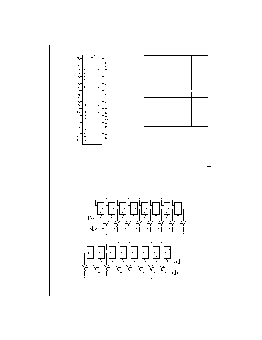
Connection Diagram
Truth Tables
H
=
HIGH Voltage Level
L
=
LOW Voltage Level
X
=
Immaterial (HIGH or LOW, control inputs may not float)
Z
=
High Impedance
O
0
=
Previous O
0
before HIGH-to-LOW of Latch Enable
Functional Description
The 74ALVCH162373 contains sixteen edge D-type
latches with 3-STATE outputs. The device is byte controlled
with each byte functioning identically, but independent of
the other. Control pins can be shorted together to obtain full
16-bit operation. The following description applies to each
byte. When the Latch Enable (LE
n
) input is HIGH, data on
the I
n
enters the latches. In this condition the latches are
transparent, i.e., a latch output will change state each time
its I input changes. When LE
n
is LOW, the latches store
information that was present on the I inputs a setup time
preceding the HIGH-to-LOW transition on LE
n
. The 3-
STATE outputs are controlled by the Output Enable (OE
n
)
input. When OE
n
is LOW the standard outputs are in the 2-
state mode. When OE
n
is HIGH, the standard outputs are
in the high impedance mode but this does not interfere with
entering new data into the latches.
Logic Diagram
Please note that this diagram is provided only for the understanding of logic operations and should not be used to estimate propagation delays.
Inputs
Outputs
LE
1
OE
1
I
0
≠I
7
O
0
≠O
7
X
H
X
Z
H
L
L
L
H
L
H
H
L
L
X
O
0
Inputs
Outputs
LE
2
OE
2
I
8
≠I
15
O
8
≠O
15
X
H
X
Z
H
L
L
L
H
L
H
H
L
L
X
O
0
3
www.fairchildsemi.com
7
4
AL
VCH16237
3
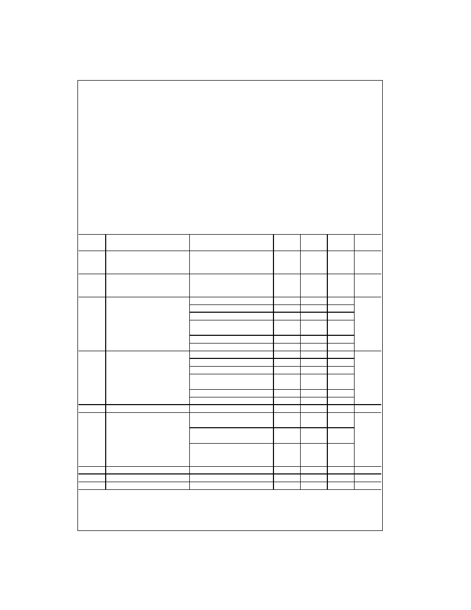
Absolute Maximum Ratings
(Note 1)
Recommended Operating
Conditions
(Note 3)
Note 1: The Absolute Maximum Ratings are those values beyond which
the safety of the device cannot be guaranteed. The device should not be
operated at these limits. The parametric values defined in the Electrical
Characteristics tables are not guaranteed at the Absolute Maximum Rat-
ings. The "Recommended Operating Conditions" table will define the condi-
tions for actual device operation.
Note 2: I
O
Absolute Maximum Rating must be observed, limited to 4.6V.
Note 3: Floating or unused control inputs must be held HIGH or LOW.
DC Electrical Characteristics
Supply Voltage (V
CC
)
-
0.5V to
+
4.6V
DC Input Voltage (V
I
)
-
0.5V to 4.6V
Output Voltage (V
O
) (Note 2)
-
0.5V to V
CC
+
0.5V
DC Input Diode Current (I
IK
)
V
I
<
0V
-
50 mA
DC Output Diode Current (I
OK
)
V
O
<
0V
-
50 mA
DC Output Source/Sink Current
(I
OH
/I
OL
)
±
50 mA
DC V
CC
or GND Current per
Supply Pin (I
CC
or GND)
±
100 mA
Storage Temperature Range (T
STG
)
-
65
∞
C to
+
150
∞
C
Power Supply
Operating
1.65V to 3.6V
Input Voltage (V
I
)
0V to V
CC
Output Voltage (V
O
)
0V to V
CC
Free Air Operating Temperature (T
A
)
-
40
∞
C to
+
85
∞
C
Minimum Input Edge Rate (
t/
V)
V
IN
=
0.8V to 2.0V, V
CC
=
3.0V
10 ns/V
Symbol
Parameter
Conditions
V
CC
Min
Max
Units
(V)
V
IH
HIGH Level Input Voltage
1.65 - 1.95
0.65 x V
CC
V
2.3 - 2.7
1.7
2.7 - 3.6
2.0
V
IL
LOW Level Input Voltage
1.65 - 1.95
0.35 x V
CC
V
2.3 - 2.7
0.7
2.7 - 3.6
0.8
V
OH
HIGH Level Output Voltage
I
OH
=
-
100
µ
A
1.65 - 3.6
V
CC
- 0.2
V
I
OH
=
-
2 mA
1.65
1.2
I
OH
=
-
4 mA
2.3
1.9
I
OH
=
-
6 mA
2.3
1.7
3.0
2.4
I
OH
=
-
8 mA
2.7
2
I
OH
=
-
12 mA
3.0
2
V
OL
LOW Level Output Voltage
I
OL
=
100
µ
A
1.65 - 3.6
0.2
V
I
OL
=
2 mA
1.65
0.45
I
OL
=
4 mA
2.3
0.4
I
OL
=
6 mA
2.3
0.55
3.0
0.55
I
OL
=
8 mA
2.7
0.6
I
OL
=
12 mA
3
0.8
I
I
Input Leakage Current
0
V
I
3.6V
3.6
±
5.0
µ
A
I
I(HOLD)
Bushold Input Minimum
V
IN
=
0.58V
1.65
25
µ
A
Drive Hold Current
V
IN
=
1.07V
1.65
-
25
V
IN
=
0.7V
2.3
45
V
IN
=
1.7V
2.3
-
45
V
IN
=
0.8V
3.0
75
V
IN
=
2.0V
3.0
-
75
0
<
V
O
3.6V
3.6
±
500
I
OZ
3-STATE Output Leakage
0
V
O
3.6V
3.6
±
10
µ
A
I
CC
Quiescent Supply Current
V
I
=
V
CC
or GND, I
O
=
0
3.6
40
µ
A
I
CC
Increase in I
CC
per Input
V
IH
=
V
CC
-
0.6V
3 - 3.6
750
µ
A

www.fairchildsemi.com
4
74
A
L
VCH162373
AC Electrical Characteristics
Capacitance
Symbol
Parameter
T
A
=
-
40
∞
C to
+
85
∞
C, R
L
=
500
Units
C
L
=
50 pF
C
L
=
30 pF
V
CC
=
3.3V
±
0.3V
V
CC
=
2.7V
V
CC
=
2.5V
±
0.2V
V
CC
=
1.8V
±
0.15V
Min
Max
Min
Max
Min
Max
Min
Max
t
PHL
, t
PLH
Propagation Delay
1.3
3.8
1.5
5.0
1.0
4.5
1.5
9.0
ns
Bus to Bus
t
PHL
, t
PLH
Propagation Delay
1.3
4.1
1.5
5.4
1.0
4.9
1.5
9.8
ns
LE to Bus
t
PZL
, t
PZH
Output Enable Time
1.3
4.4
1.5
5.9
1.0
5.4
1.5
9.8
ns
t
PLZ
, t
PHZ
Output Disable Time
1.3
4.5
1.5
4.9
1.0
4.4
1.5
7.9
ns
t
W
Pulse Width
1.5
1.5
1.5
4.0
ns
t
S
Setup Time
1.5
1.5
1.5
2.5
ns
t
H
Hold Time
1.0
1.0
1.0
1.0
ns
Symbol
Parameter
Conditions
T
A
=
+
25
∞
C
Units
V
CC
Typical
C
IN
Input Capacitance
V
I
=
0V or V
CC
3.3
6
pF
C
OUT
Output Capacitance
V
I
=
0V or V
CC
3.3
7
pF
C
PD
Power Dissipation Capacitance
Outputs Enabled f
=
10 MHz, C
L
=
50 pF
3.3
20
pF
2.5
20
5
www.fairchildsemi.com
7
4
AL
VCH16237
3
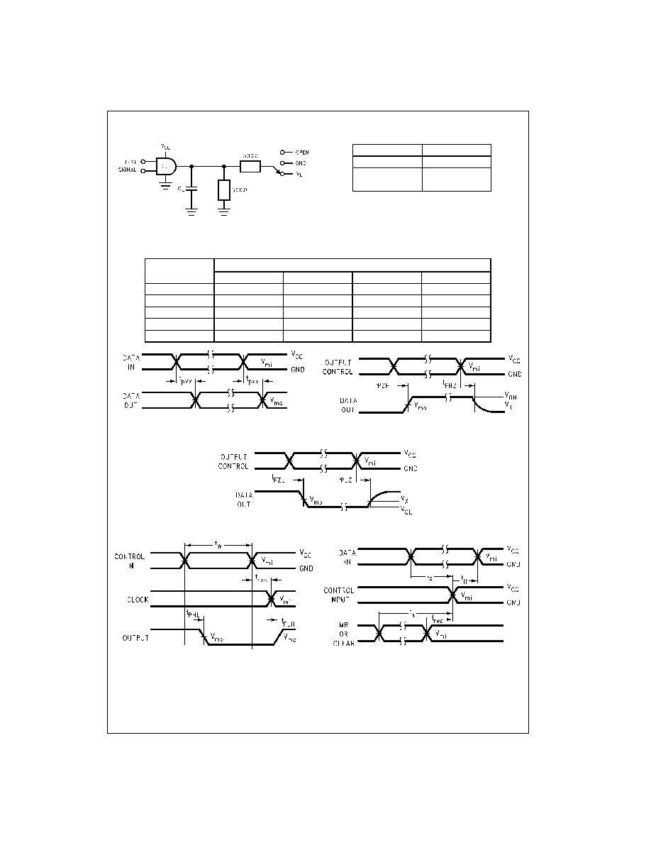
AC Loading and Waveforms
FIGURE 1. AC Test Circuit
TABLE 1. Values for Figure 1
TABLE 2. Variable Matrix
(Input Characteristics: f
=
1MHz; t
r
=
t
f
=
2ns; Z
0
=
50
)
FIGURE 2. Waveform for Inverting and
Non-Inverting Functions
FIGURE 3. 3-STATE Output HIGH Enable and
Disable Times for Low Voltage Logic
FIGURE 4. 3-STATE Output LOW Enable and Disable Times for Low Voltage Logic
FIGURE 5. Propagation Delay, Pulse Width and
t
REC
Waveforms
FIGURE 6. Setup Time, Hold Time and
Recovery Time for Low Voltage Logic
TEST
SWITCH
t
PLH
, t
PHL
Open
t
PZL
, t
PLZ
V
L
t
PZH
, t
PHZ
GND
Symbol
V
CC
3.3V
±
0.3V
2.7V
2.5V
±
0.2V
1.8V
±
0.15V
V
mi
1.5V
1.5V
V
CC
/2
V
CC
/2
V
mo
1.5V
1.5V
V
CC
/2
V
CC
/2
V
X
V
OL
+
0.3V
V
OL
+
0.3V
V
OL
+
0.15V
V
OL
+
0.15V
V
Y
V
OH
-
0.3V
V
OH
-
0.3V
V
OH
-
0.15V
V
OH
-
0.15V
V
L
6V
6V
V
CC
*2
V
CC
*2