© 2002 Fairchild Semiconductor Corporation
DS500629
www.fairchildsemi.com
September 2001
Revised February 2002
7
4
AL
VCH16240
Low
V
o
l
t
ag
e 16-
Bit
I
n
ver
ti
ng Buf
f
er
/Li
n
e
D
r
ive
r
74ALVCH16240
Low Voltage 16-Bit Inverting Buffer/Line Driver
with Bushold
General Description
The ALVCH16240 contains sixteen inverting buffers with
3-STATE outputs to be employed as a memory and
address driver, clock driver, or bus oriented transmitter/
receiver. The device is nibble (4-bit) controlled. Each nibble
has separate 3-STATE control inputs which can be shorted
together for full 16-bit operation.
The ALVCH16240 data inputs include active bushold cir-
cuitry, eliminating the need for external pull-up resistors to
hold unused or floating inputs at a valid logic level.
The 74ALVCH16240 is designed for low voltage (1.65V to
3.6V) V
CC
applications with output capability up to 3.6V.
The 74ALVCH16240 is fabricated with an advanced CMOS
technology to achieve high speed operation while maintain-
ing low CMOS power dissipation.
Features
s
1.65V to 3.6V V
CC
supply operation
s
3.6V tolerant control inputs and outputs
s
Bushold on data inputs eliminates the need for external
pull-up/pull-down resistors
s
t
PD
3.9 ns max for 3.0V to 3.6V V
CC
5.3 ns max for 2.3V to 2.7V V
CC
6.0 ns max for 1.65V to 1.95V V
CC
s
Uses patented noise/EMI reduction circuitry
s
Latch-up conforms to JEDEC JED78
s
ESD performance:
Human body model
>
2000V
Machine model
>
200V
Ordering Code:
Devices also available in Tape and Reel. Specify by appending the suffix letter "X" to the ordering code.
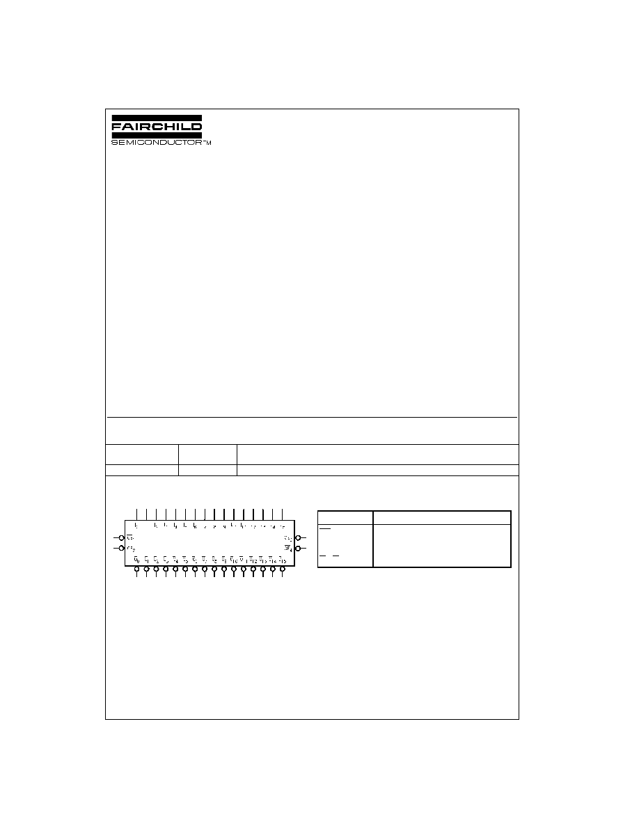
Logic Symbol
Pin Descriptions
Order Number
Package
Number
Package Descriptions
74ALVCH16240T
MTD48
48-Lead Thin Shrink Small Outline Package (TSSOP), JEDEC MO-153, 6.1mm Wide
Pin Names
Description
OE
n
Output Enable Input (Active LOW)
I
0
≠I
15
Bushold Inputs
O
0
≠O
15
Outputs
www.fairchildsemi.com
2
7
4
AL
VCH16240
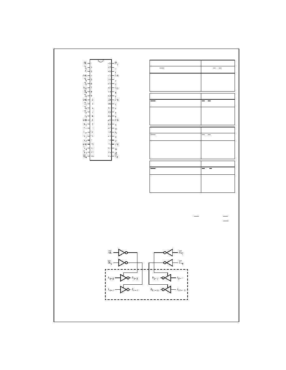
Connection Diagram
Truth Tables
H
=
HIGH Voltage Level
L
=
LOW Voltage Level
X
=
Immaterial (HIGH or LOW, inputs may not float)
Z
=
High Impedance
Functional Description
The 74ALVCH16240 contains sixteen inverting buffers with
3-STATE outputs. The device is nibble (4 bits) controlled
with each nibble functioning identically, but independent of
each other. The control pins may be shorted together to
obtain full 16-bit operation.The 3-STATE outputs are con-
trolled by an Output Enable (OE
n
) input. When OE
n
is
LOW, the outputs are in the 2-state mode. When OE
n
is
HIGH, the standard outputs are in the high impedance
mode but this does not interfere with entering new data into
the inputs.
Logic Diagram
Inputs
Outputs
OE
1
I
0
≠I
3
O
0
≠O
3
L
L
H
L
H
L
H
X
Z
Inputs
Outputs
OE
2
I
4
≠I
7
O
4
≠O
7
L
L
H
L
H
L
H
X
Z
Inputs
Outputs
OE
3
I
8
≠I
11
O
8
≠O
11
L
L
H
L
H
L
H
X
Z
Inputs
Outputs
OE
4
I
12
≠I
15
O
12
≠O
15
L
L
H
L
H
L
H
X
Z
3
www.fairchildsemi.com
7
4
AL
VCH16240
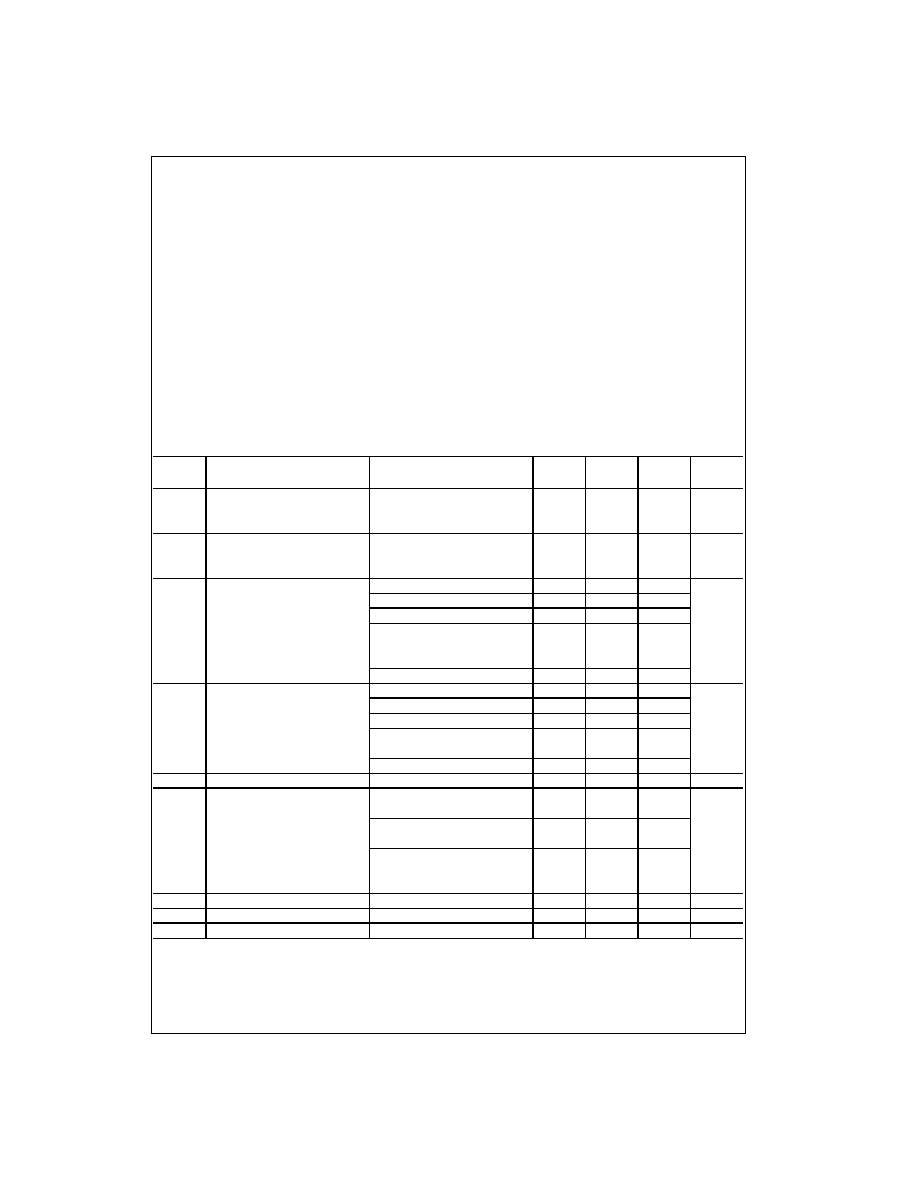
Absolute Maximum Ratings
(Note 1)
Recommended Operating
Conditions
(Note 3)
Note 1: The Absolute Maximum Ratings are those values beyond which
the safety of the device cannot be guaranteed. The device should not be
operated at these limits. The parametric values defined in the Electrical
Characteristics tables are not guaranteed at the Absolute Maximum Rat-
ings. The "Recommended Operating Conditions" table will define the condi-
tions for actual device operation.
Note 2: I
O
Absolute Maximum Rating must be observed, limited to 4.6V.
Note 3: Floating or unused control inputs must be held HIGH or LOW.
DC Electrical Characteristics
Supply Voltage (V
CC
)
-
0.5V to
+
4.6V
DC Input Voltage (V
I
)
-
0.5V to 4.6V
Output Voltage (V
O
) (Note 2)
-
0.5V to V
CC
+
0.5V
DC Input Diode Current (I
IK
)
V
I
<
0V
-
50 mA
DC Output Diode Current (I
OK
)
V
O
<
0V
-
50 mA
DC Output Source/Sink Current
(I
OH
/I
OL
)
±
50 mA
DC V
CC
or GND Current per
Supply Pin (I
CC
or GND)
±
100 mA
Storage Temperature Range (T
STG
)
-
65
∞
C to
+
150
∞
C
Power Supply
Operating
1.65V to 3.6V
Input Voltage (V
I
)
0V to V
CC
Output Voltage (V
O
)
0V to V
CC
Free Air Operating Temperature (T
A
)
-
40
∞
C to
+
85
∞
C
Minimum Input Edge Rate (
t/
V)
V
IN
=
0.8V to 2.0V, V
CC
=
3.0V
10 ns/V
Symbol
Parameter
Conditions
V
CC
Min
Max
Units
(V)
V
IH
HIGH Level Input Voltage
1.65 - 1.95
0.65 x V
CC
V
2.3 - 2.7
1.7
2.7 - 3.6
2.0
V
IL
LOW Level Input Voltage
1.65 - 1.95
0.35 x V
CC
V
2.3 - 2.7
0.7
2.7 - 3.6
0.8
V
OH
HIGH Level Output Voltage
I
OH
=
-
100
µ
A
1.65 - 3.6
V
CC
- 0.2
V
I
OH
=
-
4 mA
1.65
1.2
I
OH
=
-
6 mA
2.3
2.0
I
OH
=
-
12 mA
2.3
1.7
2.7
2.2
3.0
2.4
I
OH
=
-
24 mA
3.0
2
V
OL
LOW Level Output Voltage
I
OL
=
100
µ
A
1.65 - 3.6
0.2
V
I
OL
=
4 mA
1.65
0.45
I
OL
=
6 mA
2.3
0.4
I
OL
=
12 mA
2.3
0.7
2.7
0.4
I
OL
=
24 mA
3.0
0.55
I
I
Input Leakage Current
0
V
I
3.6V
3.6
±
5.0
µ
A
I
I(HOLD)
Bushold Input Minimum
V
IN
=
0.58V
1.65
25
µ
A
Drive Hold Current
V
IN
=
1.07V
1.65
-
25
V
IN
=
0.7V
2.3
45
V
IN
=
1.7V
2.3
-
45
V
IN
=
0.8V
3.0
75
V
IN
=
2.0V
3.0
-
75
0
<
V
O
3.6V
3.6
±
500
I
OZ
3-STATE Output Leakage
0
V
O
3.6V
3.6
±
10
µ
A
I
CC
Quiescent Supply Current
V
I
=
V
CC
or GND, I
O
=
0
3.6
40
µ
A
I
CC
Increase in I
CC
per Input
V
IH
=
V
CC
-
0.6V
3 - 3.6
750
µ
A
www.fairchildsemi.com
4
7
4
AL
VCH16240
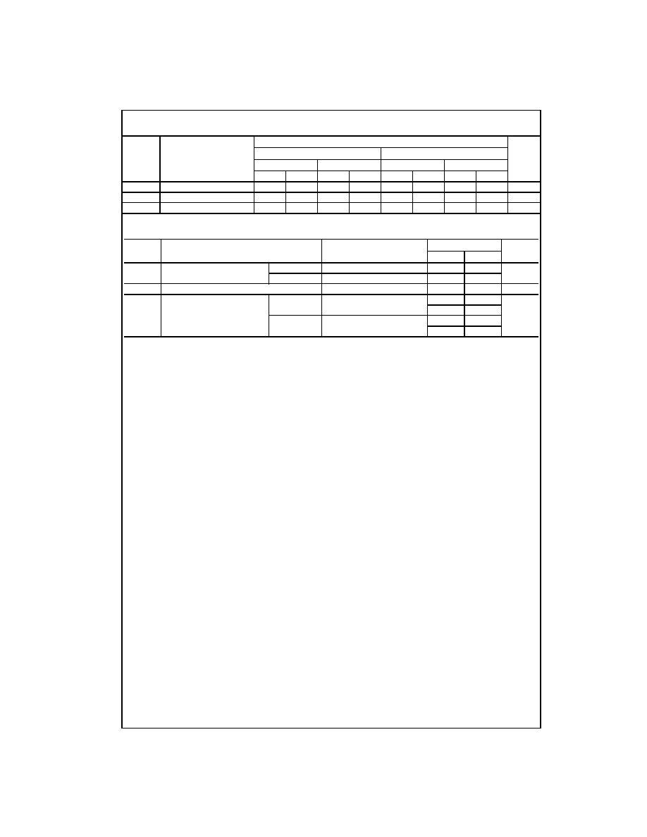
AC Electrical Characteristics
Capacitance
Symbol
Parameter
T
A
=
-
40
∞
C to
+
85
∞
C, R
L
=
500
Units
C
L
=
50 pF
C
L
=
30 pF
V
CC
=
3.3V
±
0.3V
V
CC
=
2.7V
V
CC
=
2.5V
±
0.2V
V
CC
=
1.8V
±
0.15V
Min
Max
Min
Max
Min
Max
Min
Max
t
PHL
, t
PLH
Propagation Delay
1.0
3.9
5.3
1.0
5.3
1.5
6.0
ns
t
PZL
, t
PZH
Output Enable Time
1.0
5
6.1
1.0
6.4
1.5
8.2
ns
t
PLZ
, t
PHZ
Output Disable Time
1.0
4.4
4.8
1.0
5.4
1.5
6.8
ns
Symbol
Parameter
Conditions
T
A
=
+
25
∞
C
Units
V
CC
Typical
C
IN
Input Capacitance
Control
V
I
=
0V or V
CC
3.3
3
pF
Data
V
I
=
0V or V
CC
3.3
6
C
OUT
Output Capacitance
V
I
=
0V or V
CC
3.3
7
pF
C
PD
Power Dissipation Capacitance
Outputs Enabled f
=
10 MHz, C
L
=
50 pF
3.3
19
pF
2.5
16
Outputs Disabled f
=
10 MHz, C
L
=
50 pF
3.3
5
2.5
4
5
www.fairchildsemi.com
7
4
AL
VCH16240
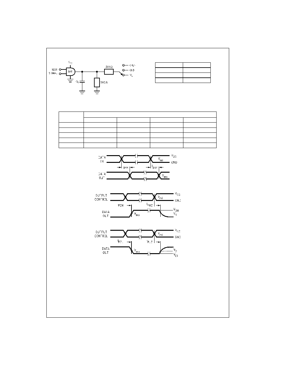
AC Loading and Waveforms
FIGURE 1. AC Test Circuit
TABLE 1. Values for Figure 1
TABLE 2. Variable Matrix
(Input Characteristics: f
=
1MHz; t
r
=
t
f
=
2ns; Z
0
=
50
)
FIGURE 2. Waveform for Inverting and Non-Inverting Functions
FIGURE 3. 3-STATE Output High Enable and Disable Times for Low Voltage Logic
FIGURE 4. 3-STATE Output Low Enable and Disable Times for Low Voltage Logic
TEST
SWITCH
t
PLH
, t
PHL
Open
t
PZL
, t
PLZ
V
L
t
PZH
, t
PHZ
GND
Symbol
V
CC
3.3V
±
0.3V
2.7V
2.5V
±
0.2V
1.8V
±
0.15V
V
mi
1.5V
1.5V
V
CC
/2
V
CC
/2
V
mo
1.5V
1.5V
V
CC
/2
V
CC
/2
V
X
V
OL
+
0.3V
V
OL
+
0.3V
V
OL
+
0.15V
V
OL
+
0.15V
V
Y
V
OH
-
0.3V
V
OH
-
0.3V
V
OH
-
0.15V
V
OH
-
0.15V
V
L
6V
6V
V
CC
*2
V
CC
*2