Äîêóìåíòàöèÿ è îïèñàíèÿ www.docs.chipfind.ru
© 2002 Fairchild Semiconductor Corporation
DS500627
www.fairchildsemi.com
September 2001
Revised February 2002
7
4
AL
VCH16374
Low
V
o
l
t
ag
e 16-
Bit
D-
T
y
pe Fl
i
p
-Fl
op wi
th
Bushol
d
74ALVCH16374
Low Voltage 16-Bit D-Type Flip-Flop with Bushold
General Description
The ALVCH16374 contains sixteen non-inverting D-type
flip-flops with 3-STATE outputs and is intended for bus ori-
ented applications. The device is byte controlled. A buff-
ered clock (CP) and output enable (OE) are common to
each byte and can be shorted together for full 16-bit opera-
tion.
The ALVCH16374 data inputs include active bushold cir-
cuitry, eliminating the need for external pull-up resistors to
hold unused or floating data inputs at a valid logic level.
The 74ALVCH16374 is designed for low voltage (1.65V to
3.6V) V
CC
applications with output compatibility up to 3.6V.
The 74ALVCH16374 is fabricated with an advanced CMOS
technology to achieve high speed operation while maintain-
ing low CMOS power dissipation.
Features
s
1.65V to 3.6V V
CC
supply operation
s
3.6V tolerant control inputs and outputs
s
Bushold on data inputs eliminates the need for external
pull-up/pull-down resistors
s
t
PD
4.2 ns max for 3.0V to 3.6V V
CC
5.3 ns max for 2.3V to 2.7V V
CC
7.8 ns max for 1.65V to 1.95V V
CC
s
Uses patented noise/EMI reduction circuitry
s
Latch-up conforms to JEDEC JED78
s
ESD performance:
Human body model
>
2000V
Machine model
>
200V
Ordering Code:
Note 1: Devices also available in Tape and Reel. Specify by appending suffix letter "X" to the ordering code.
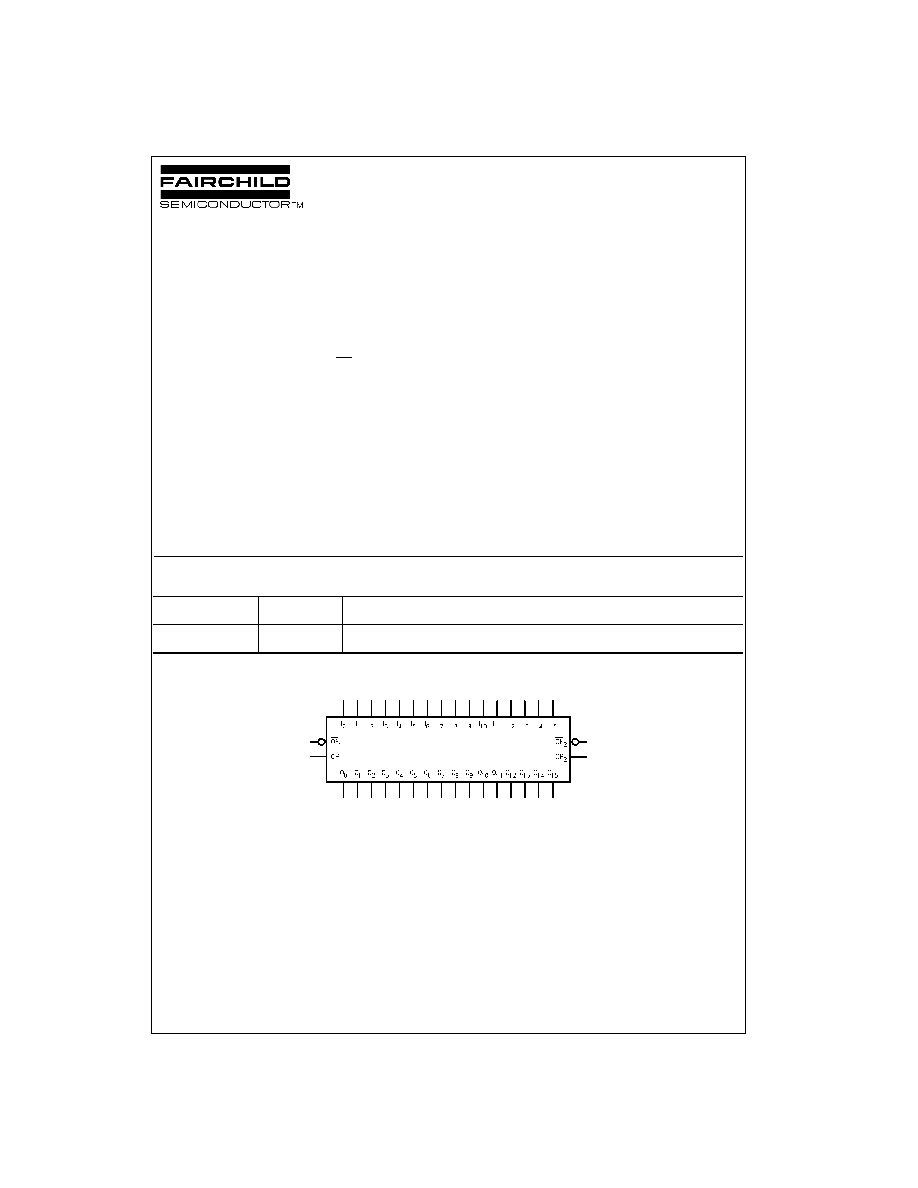
Logic Symbol
Order Number
Package
Number
Package Descriptions
74ALVCH16374T
(Note 1)
MTD48
48-Lead Thin Shrink Small Outline Package (TSSOP), JEDEC MO-153, 6.1mm Wide
www.fairchildsemi.com
2
7
4
AL
VCH16374
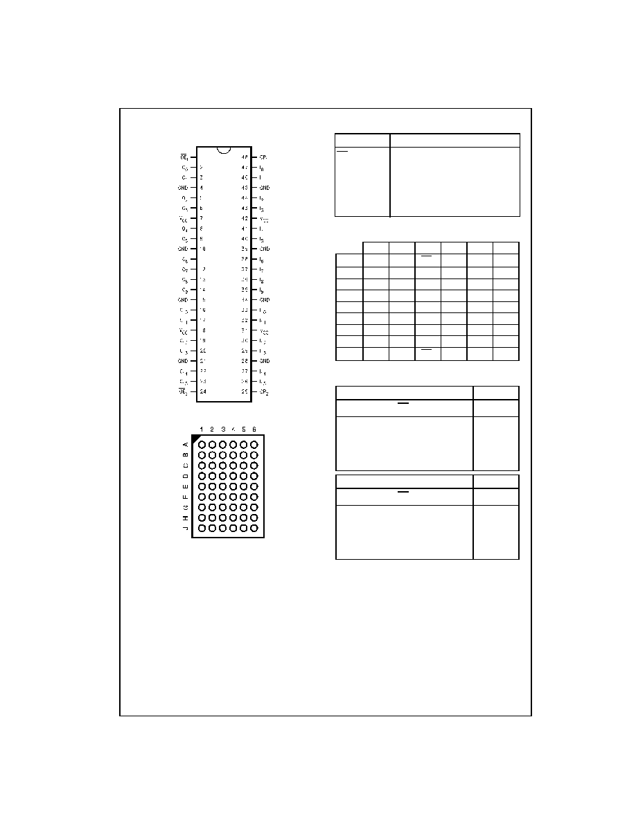
Connection Diagrams
Pin Assignment for TSSOP
Pin Assignment for FBGA
(Top Thru View)
Pin Descriptions
FBGA Pin Assignments
Truth Tables
H
=
HIGH Voltage Level
L
=
LOW Voltage Level
X
=
Immaterial (HIGH or LOW, control inputs may not float)
Z
=
High Impedance
O
0
=
Previous O
0
before HIGH-to-LOW of CP
Pin Names
Description
OE
n
Output Enable Input (Active LOW)
CP
n
Clock Pulse Input
I
0
I
15
Bushold Inputs
O
0
O
15
Outputs
NC
No Connect
1
2
3
4
5
6
A
O
0
NC
OE
1
CP
1
NC
I
0
B
O
2
O
1
NC
NC
I
1
I
2
C
O
4
O
3
V
CC
V
CC
I
3
I
4
D
O
6
O
5
GND
GND
I
5
I
6
E
O
8
O
7
GND
GND
I
7
I
8
F
O
10
O
9
GND
GND
I
9
I
10
G
O
12
O
11
V
CC
V
CC
I
11
I
12
H
O
14
O
13
NC
NC
I
13
I
14
J
O
15
NC
OE
2
CP
2
NC
I
15
Inputs
Outputs
CP
1
OE
1
I
0
I
7
O
0
O
7
L
H
H
L
L
L
L
L
X
O
0
X
H
X
Z
Inputs
Outputs
CP
2
OE
2
I
8
I
15
O
8
O
15
L
H
H
L
L
L
L
L
X
O
0
X
H
X
Z
3
www.fairchildsemi.com
7
4
AL
VCH16374
Functional Description
The 74ALVCH16374 consists of sixteen edge-triggered
flip-flops with individual D-type inputs and 3-STATE true
outputs. The device is byte controlled with each byte func-
tioning identically, but independent of the other. The control
pins can be shorted together to obtain full 16-bit operation.
Each clock has a buffered clock and buffered Output
Enable common to all flip-flops within that byte. The
description which follows applies to each byte. Each
flip-flop will store the state of their individual I inputs that
meet the setup and hold time requirements on the
LOW-to-HIGH Clock (CP
n
) transition. With the Output
Enable (OE
n
) LOW, the contents of the flip-flops are avail-
able at the outputs. When OE
n
is HIGH, the outputs go to
the high impedance state. Operations of the OE
n
input
does not affect the state of the flip-flops.
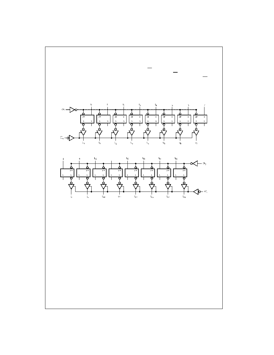
Logic Diagram
Byte 1 (0:7)
Byte 2 (8:15)
Please note that this diagram is provided only for the understanding of logic operations and should not be used to estimate propagation delays.
www.fairchildsemi.com
4
7
4
AL
VCH16374
Absolute Maximum Ratings
(Note 2)
Recommended Operating
Conditions
(Note 4)
Note 2: The Absolute Maximum Ratings are those values beyond which
the safety of the device cannot be guaranteed. The device should not be
operated at these limits. The parametric values defined in the Electrical
Characteristics tables are not guaranteed at the Absolute Maximum Rat-
ings. The "Recommended Operating Conditions" table will define the condi-
tions for actual device operation.
Note 3: I
O
Absolute Maximum Rating must be observed.
Note 4: Floating or unused control inputs must be held HIGH or LOW.
DC Electrical Characteristics
Supply Voltage (V
CC
)
-
0.5V to
+
4.6V
DC Input Voltage (V
I
)
-
0.5V to 4.6V
Output Voltage (V
O
) (Note 3)
-
0.5V to V
CC
+
0.5V
DC Input Diode Current (I
IK
)
V
I
<
0V
-
50 mA
DC Output Diode Current (I
OK
)
V
O
<
0V
-
50 mA
DC Output Source/Sink Current
(I
OH
/I
OL
)
±
50 mA
DC V
CC
or GND Current per
Supply Pin (I
CC
or GND)
±
100 mA
Storage Temperature Range (T
STG
)
-
65
°
C to
+
150
°
C
Power Supply
Operating 1.65V
to
3.6V
Input Voltage (V
I
)
0V to V
CC
Output Voltage (V
O
)
0V to V
CC
Free Air Operating Temperature (T
A
)
-
40
°
C to
+
85
°
C
Minimum Input Edge Rate (
t/
V)
V
IN
=
0.8V to 2.0V, V
CC
=
3.0V
10 ns/V
Symbol
Parameter
Conditions
V
CC
Min
Max
Units
(V)
V
IH
HIGH Level Input Voltage
1.65 - 1.95
0.65 x V
CC
V
2.3 - 2.7
1.7
2.7 - 3.6
2.0
V
IL
LOW Level Input Voltage
1.65 - 1.95
0.35 x V
CC
V
2.3 - 2.7
0.7
2.7 - 3.6
0.8
V
OH
HIGH Level Output Voltage
I
OH
=
100
µ
A
1.65 - 3.6
V
CC
- 0.2
V
I
OH
=
-
4 mA
1.65
1.2
I
OH
=
-
6 mA
2.3
2.0
I
OH
=
-
12 mA
2.3
1.7
2.7
2.2
3.0
2.4
I
OH
=
-
24 mA
3.0
2
V
OL
LOW Level Output Voltage
I
OL
=
100
µ
A
1.65 - 3.6
0.2
V
I
OL
=
4 mA
1.65
0.45
I
OL
=
6 mA
2.3
0.4
I
OL
=
12 mA
2.3
0.7
2.7
0.4
I
OL
=
24 mA
3.0
0.55
I
I
Input Leakage Current
0
V
I
3.6V
3.6
±
5.0
µ
A
I
I(HOLD)
Bushold Input Maximum
V
IN
=
0.58V
1.65
25
µ
A
Drive Hold Current
V
IN
=
1.07V
1.65
-
25
V
IN
=
0.7V
2.3
45
V
IN
=
1.7V
2.3
-
45
V
IN
=
0.8V
3.0
75
V
IN
=
2.0V
3.0
-
75
0
<
V
O
3.6V
3.6
±
500
I
OZ
3-STATE Output Leakage
0
V
O
3.6V
3.6
±
10
µ
A
I
CC
Quiescent Supply Current
V
I
=
V
CC
or GND, I
O
=
0
3.6
40
µ
A
I
CC
Increase in I
CC
per Input
V
IH
=
V
CC
-
0.6V
3 - 3.6
750
µ
A
5
www.fairchildsemi.com
7
4
AL
VCH16374
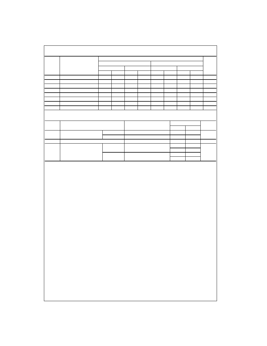
AC Electrical Characteristics
Capacitance
Symbol
Parameter
T
A
=
-
40
°
C to
+
85
°
C, R
L
=
500
Units
C
L
=
50 pF
C
L
=
30 pF
V
CC
=
3.3V
±
0.3V
V
CC
=
2.7V
V
CC
=
2.5V
±
0.2V
V
CC
=
1.8V
±
0.15V
Min
Max
Min
Max
Min
Max
Min
Max
f
CLOCK
Clock Frequency
150
150
150
100
MHz
t
W
Pulse Width
3.3
3.3
3.3
4.0
ns
t
S
Setup Time
1.9
2.2
2.1
2.5
ns
t
H
Hold Time
0.5
0.5
0.6
1.0
ns
f
MAX
Maximum Clock Frequency
150
150
150
100
MHz
t
PHL
, t
PLH
Propagation Delay
1.0
4.2
4.9
1.0
5.3
1.5
7.8
ns
t
PZL
, t
PZH
Output Enable Time
1.0
4.8
5.9
1.0
6.2
1.5
9.2
ns
t
PLZ
, t
PHZ
Output Disable Time
1.0
4.3
4.7
1.0
5.3
1.5
6.8
ns
Symbol
Parameter
Conditions
T
A
=
+
25
°
C
Units
V
CC
Typical
C
IN
Input Capacitance
Control
V
I
=
0V or V
CC
3.3
3
pF
Data
V
I
=
0V or V
CC
3.3
6
C
OUT
Output Capacitance
V
I
=
0V or V
CC
3.3
7
pF
C
PD
Power Dissipation Capacitance
Outputs Enabled f
=
10 MHz, C
L
=
50 pF
3.3
30
pF
2.5
31
Outputs Disabled f
=
10 MHz, C
L
=
50 pF
3.3
18
2.5
16