 | –≠–ª–µ–∫—Ç—Ä–æ–Ω–Ω—ã–π –∫–æ–º–ø–æ–Ω–µ–Ω—Ç: 74C00 | –°–∫–∞—á–∞—Ç—å:  PDF PDF  ZIP ZIP |

October 1987
Revised January 1999
MM74C00
∑ MM74C02
∑
MM
7
4
C04 Quad
2-I
nput
NAND Gat
e
∑
Quad 2
-
I
nput
NO
R
Gate
∑ He
x I
n
ver
t
e
r
© 1999 Fairchild Semiconductor Corporation
DS005877.prf
www.fairchildsemi.com
MM74C00 ∑ MM74C02 ∑ MM74C04
Quad 2-Input NAND Gate ∑
Quad 2-Input NOR Gate ∑
Hex Inverter
General Description
The MM74C00, MM74C02, and MM74C04 logic gates
employ complementary MOS (CMOS) to achieve wide
power supply operating range, low power consumption,
high noise immunity and symmetric controlled rise and fall
times. With features such as this the 74C logic family is
close to ideal for use in digital systems. Function and pin
out compatibility with series 74 devices minimizes design
time for those designers already familiar with the standard
74 logic family.
All inputs are protected from damage due to static dis-
charge by diode clamps to V
CC
and GND.
Features
s
Wide supply voltage range:
3V to 15V
s
Guaranteed noise margin:
1V
s
High noise immunity:
0.45 V
CC
(typ.)
s
Low power consumption:
10 nW/package (typ.)
s
Low power:
TTL compatibility:
Fan out of 2 driving 74L
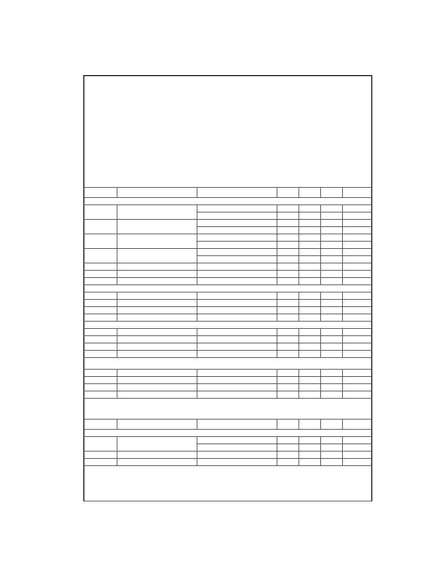
Ordering Code:
Device also available in Tape and Reel. Specify by appending suffix letter "X" to the ordering code.
Connection Diagrams
Pin Assignments for DIP and SOIC
MM74C00
Top View
MM74C02
Top View
MM74C04
Top View
Order Number
Package Number
Package Description
MM74C00M
M14A
14-Lead Small Outline Integrated Circuit (SOIC), JEDEC MS-120, 0.150" Narrow
MM74C00N
N14A
14-Lead Plastic Dual-In-Line Package (PDIP), JEDEC MS-001, 0.300" Wide
MM74C02N
M14A
14-Lead Small Outline Integrated Circuit (SOIC), JEDEC MS-120, 0.150" Narrow
MM74C04M
M14A
14-Lead Small Outline Integrated Circuit (SOIC), JEDEC MS-120, 0.150" Narrow
MM74C04N
N14A
14-Lead Plastic Dual-In-Line Package (PDIP), JEDEC MS-001, 0.300" Wide
www.fairchildsemi.com
2
MM74C00
∑
MM74C02
∑ MM
74C04
Absolute Maximum Ratings
(Note 1)
Note 1: "Absolute Maximum Ratings" are those values beyond which the
safety of the device cannot be guaranteed. Except for "Operating Tempera-
ture Range" they are not meant to imply that the devices should be oper-
ated at these limits. The table of "Electrical Characteristics" provides
conditions for actual device operation.
DC Electrical Characteristics
Min/Max limits apply across the guaranteed temperature range unless otherwise noted
AC Electrical Characteristics
(Note 2)
T
A
=
25
∞
C, C
L
=
50 pF, unless otherwise specified
Note 2: AC Parameters are guaranteed by DC correlated testing.
Note 3: Capacitance is guaranteed by periodic testing.
Note 4: C
PD
determines the no load AC power consumption of any CMOS device. For complete explanation see Family Characteristics Application Note--
AN-90.
Voltage at Any Pin
-
0.3V to V
CC
+
0.3V
Operating Temperature Range
-
40
∞
C to
+
85
∞
C
Storage Temperature Range
-
65
∞
C to
+
150
∞
C
Operating V
CC
Range
3.0V to 15V
Maximum V
CC
Voltage
18V
Power Dissipation (P
D
)
Dual-In-Line
700 mW
Small Outline
500 mW
Lead Temperature
(Soldering, 10 seconds)
300
∞
C
Symbol
Parameter
Conditions
Min
Typ
Max
Units
CMOS TO CMOS
V
IN(1)
Logical "1" Input Voltage
V
CC
=
5.0V
3.5
V
V
CC
=
10V
8.0
V
V
IN(0)
Logical "0" Input Voltage
V
CC
=
5.0V
1.5
V
V
CC
=
10V
2.0
V
V
OUT(1)
Logical "1" Output Voltage
V
CC
=
5.0V, I
O
=
-
10
µ
A
4.5
V
V
CC
=
10V, I
O
=
-
10
µ
A
9.0
V
V
OUT(0)
Logical "0" Output Voltage
V
CC
=
5.0V, I
O
=
10
µ
A
0.5
V
V
CC
=
10V, I
O
=
10
µ
A
1.0
V
I
IN(1)
Logical "1" Input Current
V
CC
=
15V, V
IN
=
15V
0.005
1.0
µ
A
I
IN(0)
Logical "0" Input Current
V
CC
=
15V, V
IN
=
0V
-
1.0
-
0.005
µ
A
I
CC
Supply Current
V
CC
=
15V
0.01
15
µ
A
LOW POWER TO CMOS
V
IN(1)
Logical "1" Input Voltage
74C, V
CC
=
4.75V
V
CC
-
1.5
V
V
IN(0)
Logical "0" Input Voltage
74C, V
CC
=
4.75V
0.8
V
V
OUT(1)
Logical "1" Output Voltage
74C, V
CC
=
4.75V, I
O
=
-
10
µ
A
4.4
V
V
OUT(0)
Logical "0" Output Voltage
74C, V
CC
=
4.75V, I
O
=
10
µ
A
0.4
V
CMOS TO LOW POWER
V
IN(1)
Logical "1" Input Voltage
74C, V
CC
=
4.75V
4.0
V
V
IN(0)
Logical "0" Input Voltage
74C, V
CC
=
4.75V
1.0
V
V
OUT(1)
Logical "1" Output Voltage
74C, V
CC
=
4.75V, I
O
=
-
360
µ
A
2.4
V
V
OUT(0)
Logical "0" Output Voltage
74C, V
CC
=
4.75V, I
O
=
360
µ
A
0.4
V
OUTPUT DRIVE (see Family Characteristics Data Sheet) T
A
=
25
∞
C (short circuit current)
I
SOURCE
Output Source Current
V
CC
=
5.0V, V
IN(0)
=
0V, V
OUT
=
0V
-
1.75
mA
I
SOURCE
Output Source Current
V
CC
=
10V, V
IN(0)
=
0V, V
OUT
=
0V
-
8.0
mA
I
SINK
Output Sink Current
V
CC
=
5.0V, V
IN(1)
=
5.0V, V
OUT
=
V
CC
1.75
mA
I
SINK
Output Sink Current
V
CC
=
10V, V
IN(1)
=
10V, V
OUT
=
V
CC
8.0
mA
Symbol
Parameter
Conditions
Min
Typ
Max
Units
MM74C00, MM74C02, MM74C04
t
pd0
, t
pd1
Propagation Delay Time to
V
CC
=
5.0V
50
90
ns
Logical "1" or "0"
V
CC
=
10V
30
60
ns
C
IN
Input Capacitance
(Note 3)
6.0
pF
C
PD
Power Dissipation Capacitance
Per Gate or Inverter (Note 4)
12
pF
3
www.fairchildsemi.com
MM74C00
∑
MM74C02 ∑
MM
7
4
C04
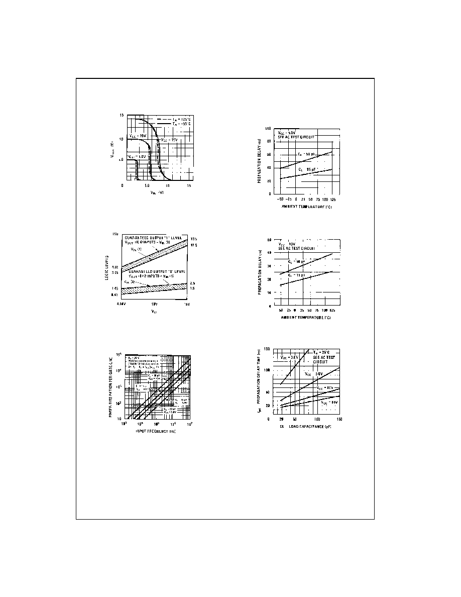
Typical Performance Characteristics
Gate Transfer Characteristics
Guaranteed Noise Margin
Over Temperature vs V
CC
Power Dissipation vs Frequency
MM74C00, MM74C02, MM74C04
Propagation Delay vs
Ambient Temperature
MM74C00, MM74C02, MM74C04
Propagation Delay vs
Ambient Temperature
MM74C00, MM74C02, MM74C04
Propagation Delay Time vs
Load Capacitance
MM74C00, MM74C02, MM74C04
www.fairchildsemi.com
4
MM74C00
∑
MM74C02
∑ MM
74C04
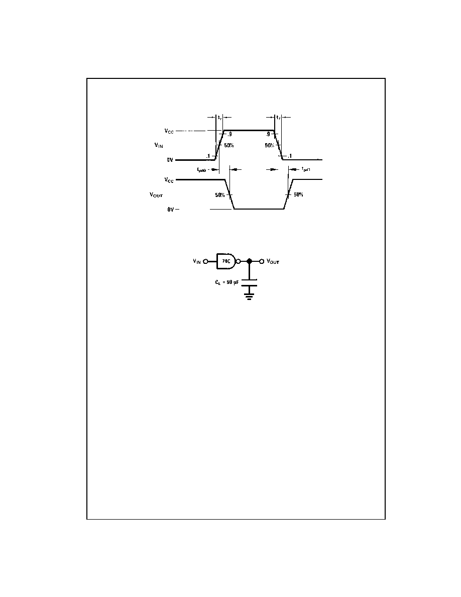
Switching Time Waveforms and AC Test Circuit
CMOS to CMOS
Delays measured with input t
r
, t
f
20 ns.
5
www.fairchildsemi.com
MM74C00
∑
MM74C02 ∑
MM
7
4
C04
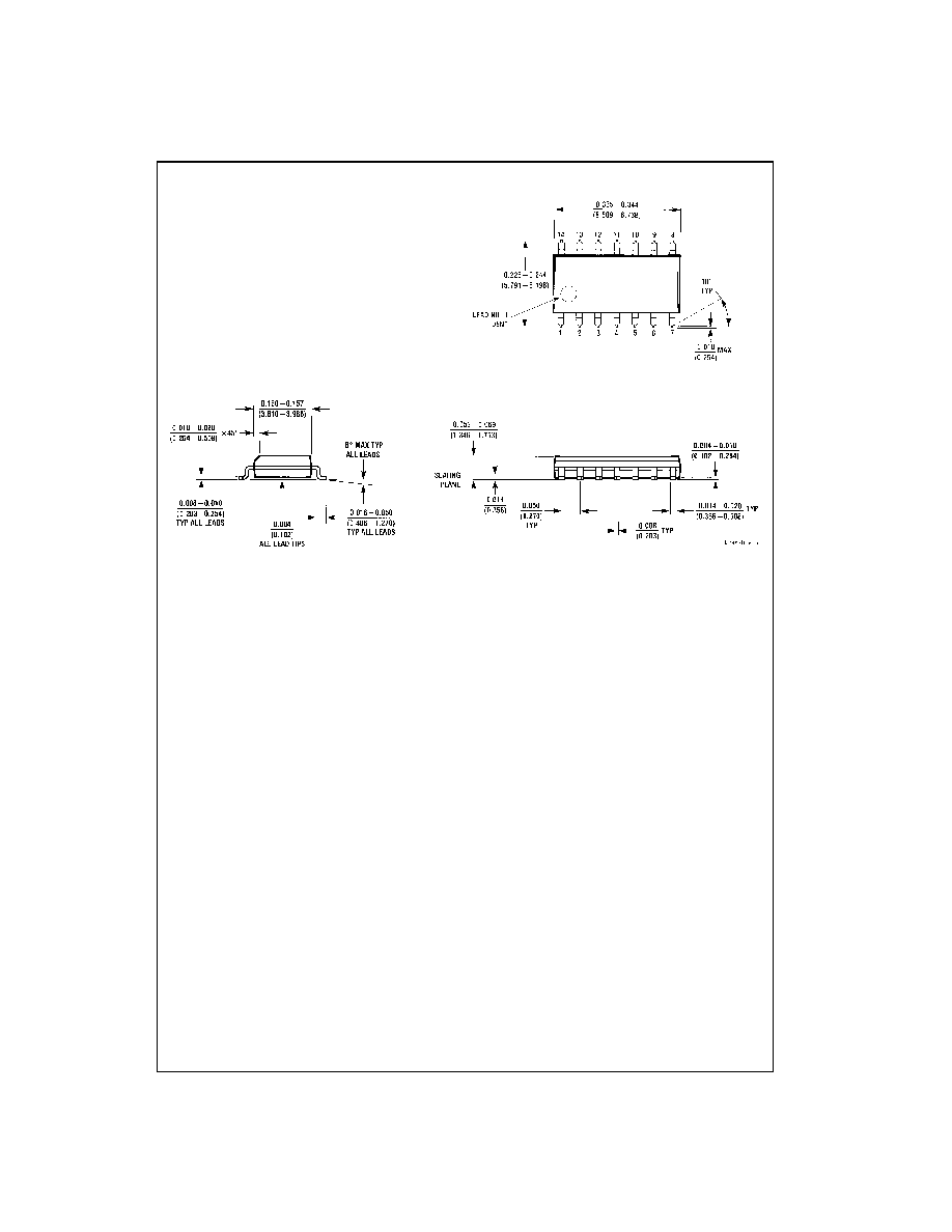
Physical Dimensions
inches (millimeters) unless otherwise noted
14-Lead Small Outline Integrated Circuit (SOIC), JEDEC MS-120, 0.150" Narrow
Package Number M14A