 | –≠–ª–µ–∫—Ç—Ä–æ–Ω–Ω—ã–π –∫–æ–º–ø–æ–Ω–µ–Ω—Ç: 74C923 | –°–∫–∞—á–∞—Ç—å:  PDF PDF  ZIP ZIP |
October 1987
Revised January 1999
MM74C922
∑
MM74C923 16-K
e
y Encoder ∑ 20-K
e
y Encoder
© 1999 Fairchild Semiconductor Corporation
DS006037.prf
www.fairchildsemi.com
MM74C922 ∑ MM74C923
16-Key Encoder ∑ 20-Key Encoder
General Description
The MM74C922 and MM74C923 CMOS key encoders pro-
vide all the necessary logic to fully encode an array of
SPST switches. The keyboard scan can be implemented
by either an external clock or external capacitor. These
encoders also have on-chip pull-up devices which permit
switches with up to 50 k
on resistance to be used. No
diodes in the switch array are needed to eliminate ghost
switches. The internal debounce circuit needs only a single
external capacitor and can be defeated by omitting the
capacitor. A Data Available output goes to a high level
when a valid keyboard entry has been made. The Data
Available output returns to a low level when the entered
key is released, even if another key is depressed. The Data
Available will return high to indicate acceptance of the new
key after a normal debounce period; this two-key roll-over
is provided between any two switches.
An internal register remembers the last key pressed even
after the key is released. The 3-STATE outputs provide for
easy expansion and bus operation and are LPTTL compat-
ible.
Features
s
50 k
maximum switch on resistance
s
On or off chip clock
s
On-chip row pull-up devices
s
2 key roll-over
s
Keybounce elimination with single capacitor
s
Last key register at outputs
s
3-STATE output LPTTL compatible
s
Wide supply range:
3V to 15V
s
Low power consumption
Ordering Code:
Device also available in Tape and Reel. Specify by appending suffix letter "X" to the ordering code.
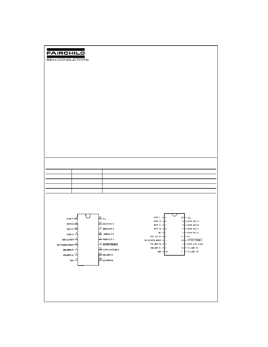
Connection Diagrams
Pin Assignment for DIP
Top View
MM94C922
Pin Assignment for SOIC
Top View
MM74C922
Order Number
Package Number
Package Description
MM74C922N
N18A
18-Lead Plastic Dual-In-Line Package (PDIP), JEDEC MS-001, 0.300" Wide
MM74C922WM
M20B
20-Lead Small Outline Integrated Circuit (SOIC), JEDEC MS-013, 0.300" Wide
MM74C923WM
M20B
20-Lead Small Outline Integrated Circuit (SOIC), JEDEC MS-013, 0.300" Wide
MM74C923N
N20A
20-Lead Plastic Dual-In-Line Package (PDIP), JEDEC MS-001, 0.300" Wide
www.fairchildsemi.com
2
MM
74
C
9
2
2
∑ M
M
74C923
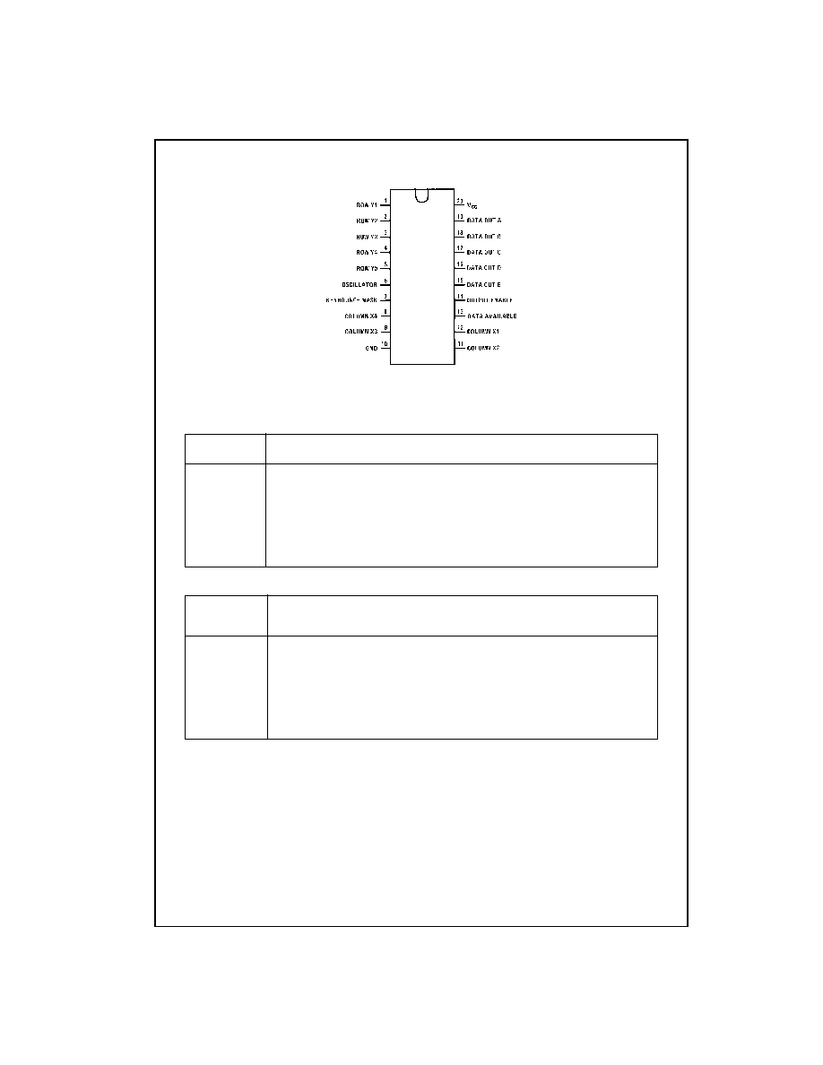
Connection Diagrams
(Continued)
Pin Assignment for
DIP and SOIC Package
Top View
MM74C923
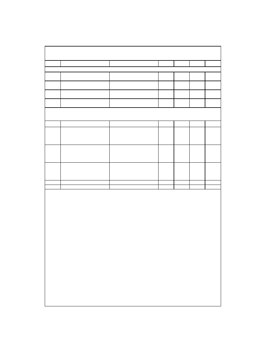
Truth Tables
(Pins 0 through 11)
(Pins 12 through 19)
Note 1: Omit for MM74C922
Switch
Position
0
1
2
3
4
5
6
7
8
9
10
11
Y1,X1 Y1,X2 Y1,X3 Y1,X4 Y2,X1 Y2,X2 Y2,X3 Y2,X4 Y3,X1 Y3,X2 Y3,X3 Y3,X4
D
A
A
0
1
0
1
0
1
0
1
0
1
0
1
T
B
0
0
1
1
0
0
1
1
0
0
1
1
A
C
0
0
0
0
1
1
1
1
0
0
0
0
O
D
0
0
0
0
0
0
0
0
1
1
1
1
U
E
(Note 1)
0
0
0
0
0
0
0
0
0
0
0
0
T
Switch
Position
12
13
14
15
16
17
18
19
Y4,X1
Y4,X2
Y4,X3
Y4,X4
Y5(Note 1),
X1
Y5 (Note 1),
X2
Y5 (Note 1),
X3
Y5 (Note 1),
X4
D
A
A
0
1
0
1
0
1
0
1
T
B
0
0
1
1
0
0
1
1
A
C
1
1
1
1
0
0
0
0
O
D
1
1
1
1
0
0
0
0
U
E
(Note 1)
0
0
0
0
1
1
1
1
T
3
www.fairchildsemi.com
MM74C922
∑ MM74C923
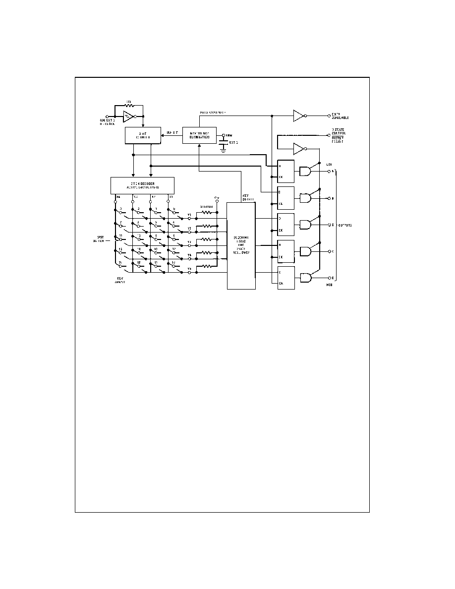
Block Diagram
www.fairchildsemi.com
4
MM
74
C
9
2
2
∑ M
M
74C923
Absolute Maximum Ratings
(Note 2)
Note 2: "Absolute Maximum Ratings" are those values beyond which the
safety of the device cannot be guaranteed. Except for "Operating Tempera-
ture Range" they are not meant to imply that the devices should be oper-
ated at these limits. The table of "Electrical Characteristics" provides
conditions for actual device operation.
DC Electrical Characteristics
Min/Max limits apply across temperature range unless otherwise specified
Voltage at Any Pin
V
CC
-
0.3V to V
CC
+
0.3V
Operating Temperature Range
MM74C922,
MM74C923
-
40
∞
C to
+
85
∞
C
Storage Temperature Range
-
65
∞
C to
+
150
∞
C
Power Dissipation (P
D
)
Dual-In-Line 700
mW
Small Outline
500 mW
Operating V
CC
Range
3V to 15V
V
CC
18V
Lead Temperature
(Soldering, 10 seconds)
260
∞
C
Symbol
Parameter
Conditions
Min
Typ
Max
Units
CMOS TO CMOS
V
T
+
Positive-Going Threshold Voltage
V
CC
=
5V, I
IN
0.7 mA
3.0
3.6
4.3
V
at Osc and KBM Inputs
V
CC
=
10V, I
IN
1.4 mA
6.0
6.8
8.6
V
V
CC
=
15V, I
IN
2.1 mA
9.0
10
12.9
V
V
T
-
Negative-Going Threshold Voltage
V
CC
=
5V, I
IN
0.7 mA
0.7
1.4
2.0
V
at Osc and KBM Inputs
V
CC
=
10V, I
IN
1.4 mA
1.4
3.2
4.0
V
V
CC
=
15V, I
IN
2.1 mA
2.1
5
6.0
V
V
IN(1)
Logical "1" Input Voltage,
V
CC
=
5V
3.5
4.5
V
Except Osc and KBM Inputs
V
CC
=
10V
8.0
9
V
V
CC
=
15V
12.5
13.5
V
V
IN(0)
Logical "0" Input Voltage,
V
CC
=
5V
0.5
1.5
V
Except Osc and KBM Inputs
V
CC
=
10V
1
2
V
V
CC
=
15V
1.5
2.5
V
I
rp
Row Pull-Up Current at Y1, Y2,
V
CC
=
5V, V
IN
=
0.1 V
CC
-
2
-
5
µ
A
Y3, Y4 and Y5 Inputs
V
CC
=
10V
-
10
-
20
µ
A
V
CC
=
15V
-
22
-
45
µ
A
V
OUT(1)
Logical "1" Output Voltage
V
CC
=
5V, I
O
=
-
10
µ
A
4.5
V
V
CC
=
10V, I
O
=
-
10
µ
A
9
V
V
CC
=
15V, I
O
=
-
10
µ
A
13.5
V
V
OUT(0)
Logical "0" Output Voltage
V
CC
=
5V, I
O
=
10
µ
A
0.5
V
V
CC
=
10V, I
O
=
10
µ
A
1
V
V
CC
=
15V, I
O
=
10
µ
A
1.5
V
R
on
Column "ON" Resistance at
V
CC
=
5V, V
O
=
0.5V
500
1400
X1, X2, X3 and X4 Outputs
V
CC
=
10V, V
O
=
1V
300
700
V
CC
=
15V, V
O
=
1.5V
200
500
I
CC
Supply Current
V
CC
=
5V
0.55
1.1
mA
Osc at 0V, (one Y low)
V
CC
=
10V
1.1
1.9
mA
V
CC
=
15V
1.7
2.6
mA
I
IN(1)
Logical "1" Input Current
V
CC
=
15V, V
IN
=
15V
0.005
1.0
µ
A
at Output Enable
I
IN(0)
Logical "0" Input Current
V
CC
=
15V, V
IN
=
0V
-
1.0
-
0.005
µ
A
at Output Enable
CMOS/LPTTL INTERFACE
V
IN(1)
Except Osc and KBM Inputs
V
CC
=
4.75V
V
CC
-
1.5
V
V
IN(0)
Except Osc and KBM Inputs
V
CC
=
4.75V
0.8
V
V
OUT(1)
Logical "1" Output Voltage
I
O
=
-
360
µ
A
V
CC
=
4.75V
2.4
V
I
O
=
-
360
µ
A
V
OUT(0)
Logical "0" Output Voltage
I
O
=
-
360
µ
A
V
CC
=
4.75V
0.4
V
I
O
=
-
360
µ
A
5
www.fairchildsemi.com
MM74C922
∑ MM74C923
DC Electrical Characteristics
(Continued)
AC Electrical Characteristics
(Note 3)
T
A
=
25
∞
C, C
L
=
50 pF, unless otherwise noted
Note 3: AC Parameters are guaranteed by DC correlated testing.
Note 4: Capacitance is guaranteed by periodic testing.
Symbol
Parameter
Conditions
Min
Typ
Max
Units
OUTPUT DRIVE (See Family Characteristics Data Sheet) (Short Circuit Current)
I
SOURCE
Output Source Current
V
CC
=
5V, V
OUT
=
0V,
-
1.75
-
3.3
mA
(P-Channel)
T
A
=
25
∞
C
I
SOURCE
Output Source Current
V
CC
=
10V, V
OUT
=
0V,
-
8
-
15 mA
(P-Channel)
T
A
=
25
∞
C
I
SINK
Output Sink Current
V
CC
=
5V, V
OUT
=
V
CC
,
1.75
3.6
mA
(N-Channel)
T
A
=
25
∞
C
I
SINK
Output Sink Current
V
CC
=
10V, V
OUT
=
V
CC
,
8
16
mA
(N-Channel)
T
A
=
25
∞
C
Symbol
Parameter
Conditions
Min
Typ
Max
Units
t
pd0
, t
pd1
Propagation Delay Time to
C
L
=
50 pF (Figure 1)
Logical "0" or Logical "1"
V
CC
=
5V
60
150
ns
from D.A.
V
CC
=
10V
35
80
ns
V
CC
=
15V
25
60
ns
t
0H
, t
1H
Propagation Delay Time from
R
L
=
10k, C
L
=
10 pF (Figure 2)
Logical "0" or Logical "1"
V
CC
=
5V, R
L
=
10k
80
200
ns
into High Impedance State
V
CC
=
10V, C
L
=
10 pF
65
150
ns
V
CC
=
15V
50
110
ns
t
H0
, t
H1
Propagation Delay Time from
R
L
=
10k, C
L
=
50 pF (Figure 2)
High Impedance State to a
V
CC
=
5V, R
L
=
10k
100
250
ns
Logical "0" or Logical "1"
V
CC
=
10V, C
L
=
50 pF
55
125
ns
V
CC
=
15V
40
90
ns
C
IN
Input Capacitance
Any Input (Note 4)
5
7.5
pF
C
OUT
3-STATE Output Capacitance
Any Output (Note 4)
10
pF