 | –≠–ª–µ–∫—Ç—Ä–æ–Ω–Ω—ã–π –∫–æ–º–ø–æ–Ω–µ–Ω—Ç: 74F112SJ | –°–∫–∞—á–∞—Ç—å:  PDF PDF  ZIP ZIP |
© 1999 Fairchild Semiconductor Corporation
DS009472
www.fairchildsemi.com
April 1988
Revised July 1999
7
4
F1
1
2
Dua
l J
K
Ne
ga
t
i
v
e
E
dge
-
T
rigge
re
d Fli
p-
Fl
op
74F112
Dual JK Negative Edge-Triggered Flip-Flop
General Description
The 74F112 contains two independent, high-speed JK flip-
flops with Direct Set and Clear inputs. Synchronous state
changes are initiated by the falling edge of the clock. Trig-
gering occurs at a voltage level of the clock and is not
directly related to the transition time. The J and K inputs
can change when the clock is in either state without affect-
ing the flip-flop, provided that they are in the desired state
during the recommended setup and hold times relative to
the falling edge of the clock. A LOW signal on S
D
or C
D
prevents clocking and forces Q or Q HIGH, respectively.
Simultaneous LOW signals on S
D
and C
D
force both Q and
Q HIGH.
Asynchronous Inputs:
LOW input to S
D
sets Q to HIGH level
LOW input to C
D
sets Q to LOW level
Clear and Set are independent of clock
Simultaneous LOW on C
D
and S
D
makes both Q
and Q HIGH
Ordering Code:
Devices also available in Tape and Reel. Specify by appending the suffix letter "X" to the ordering code.
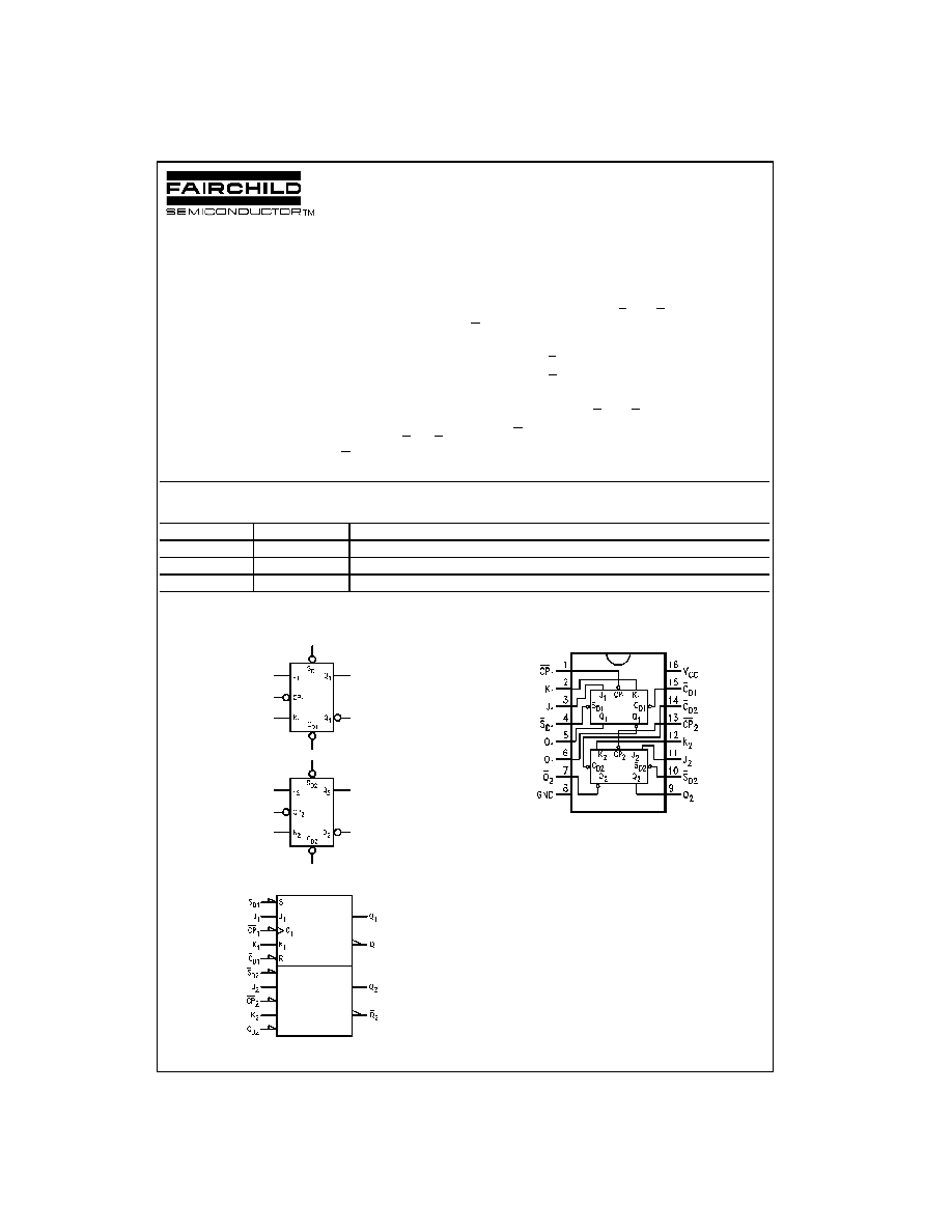
Logic Symbols
IEEE/IEC
Connection Diagram
Order Number
Package Number
Package Description
74F112SC
M16A
16-Lead Small Outline Integrated Circuit (SOIC), JEDEC MS-012, 0.150 Narrow
74F112SJ
M16D
16-Lead Small Outline Package (SOP), EIAJ TYPE II, 5.3mm Wide
74F112PC
N16E
16-Lead Plastic Dual-In-Line Package (PDIP), JEDEC MS-001, 0.300 Wide
www.fairchildsemi.com
2
74
F
1
12
Unit Loading/Fan Out
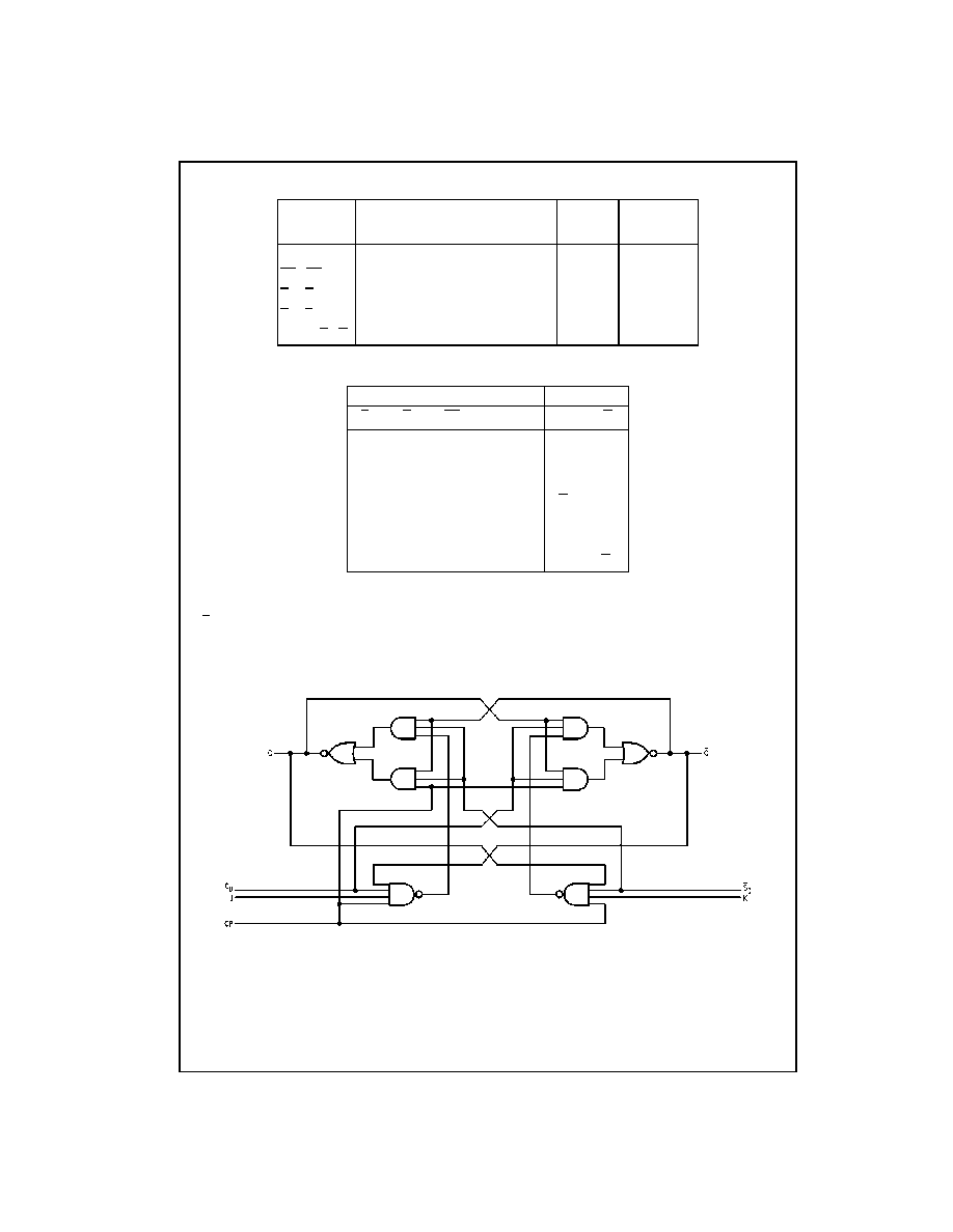
Truth Table
H (h)
=
HIGH Voltage Level
L (l)
=
LOW Voltage Level
X
=
Immaterial
=
HIGH-to-LOW Clock Transition
Q
0
(Q
0
)
=
Before HIGH-to-LOW Transition of Clock
Lower case letters indicate the state of the referenced input or output one setup time prior to the HIGH-to-LOW clock transition.
Logic Diagram
(One Half Shown)
Please note that this diagram is provided only for the understanding of logic operations and should not be used to estimate propagation delays.
Pin Names
Description
U.L.
Input I
IH
/I
IL
HIGH/LOW Output I
OH
/I
OL
J
1
, J
2
, K
1
, K
2
Data Inputs
1.0/1.0
20
µ
A/
-
0.6 mA
CP
1
, CP
2
Clock Pulse Inputs (Active Falling Edge)
1.0/4.0
20
µ
A/
-
2.4 mA
C
D1
, C
D2
Direct Clear Inputs (Active LOW)
1.0/5.0
20
µ
A/
-
3.0 mA
S
D1
, S
D2
Direct Set Inputs (Active LOW)
1.0/5.0
20
µ
A/
-
3.0 mA
Q
1
, Q
2
, Q
1
, Q
2
Outputs
50/33.3
-
1 mA/20 mA
Inputs
Outputs
S
D
C
D
CP
J
K
Q
Q
L
H
X
X
X
H
L
H
L
X
X
X
L
H
L
L
X
X
X
H
H
H
H
h
h
Q
0
Q
0
H
H
l
h
L
H
H
H
h
l
H
L
H
H
l
l
Q
0
Q
0
3
www.fairchildsemi.com
74
F
1
12
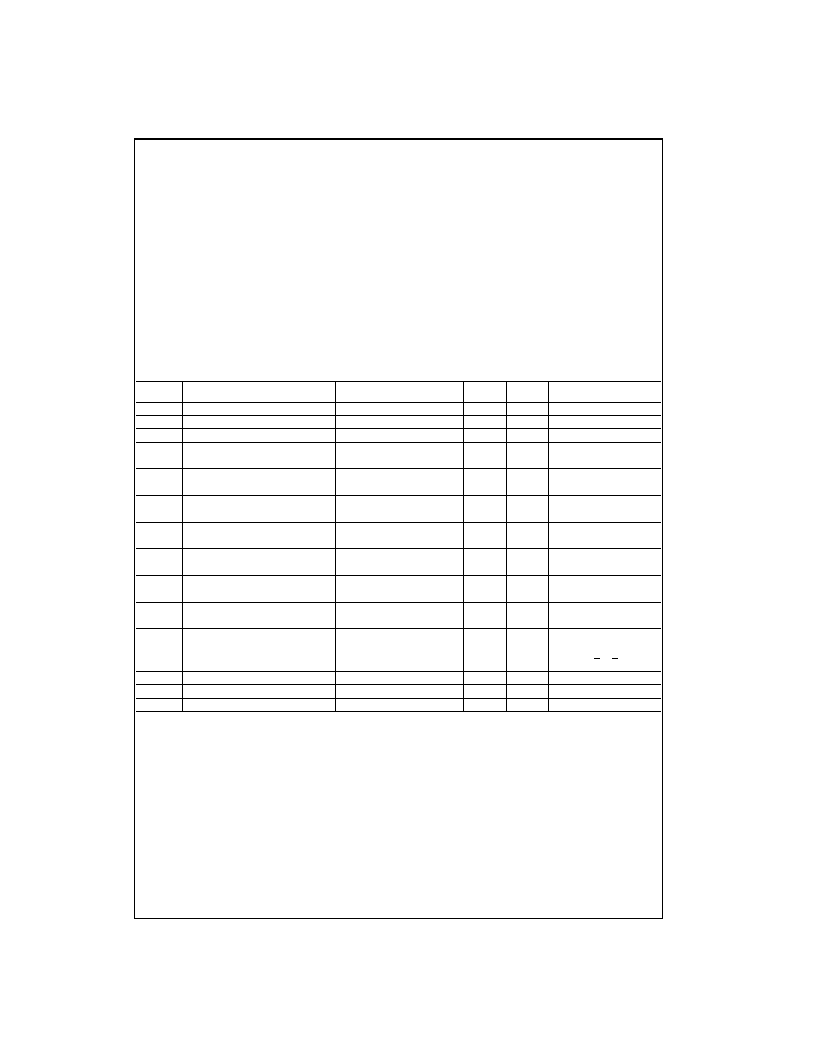
Absolute Maximum Ratings
(Note 1)
Recommended Operating
Conditions
Note 1: Absolute maximum ratings are values beyond which the device
may be damaged or have its useful life impaired. Functional operation
under these conditions is not implied.
Note 2: Either voltage limit or current limit is sufficient to protect inputs.
DC Electrical Characteristics
Storage Temperature
-
65
∞
C to
+
150
∞
C
Ambient Temperature under Bias
-
55
∞
C to
+
125
∞
C
Junction Temperature under Bias
-
55
∞
C to
+
150
∞
C
V
CC
Pin Potential to Ground Pin
-
0.5V to
+
7.0V
Input Voltage (Note 2)
-
0.5V to
+
7.0V
Input Current (Note 2)
-
30 mA to
+
5.0 mA
Voltage Applied to Output
in HIGH State (with V
CC
=
0V)
Standard Output
-
0.5V to V
CC
3-STATE Output
-
0.5V to
+
5.5V
Current Applied to Output
in LOW State (Max)
twice the rated I
OL
(mA)
Free Air Ambient Temperature
0
∞
C to
+
70
∞
C
Supply Voltage
+
4.5V to
+
5.5V
Symbol
Parameter
Min
Typ
Max
Units
V
CC
Conditions
V
IH
Input HIGH Voltage
2.0
V
Recognized as a HIGH Signal
V
IL
Input LOW Voltage
0.8
V
Recognized as a LOW Signal
V
CD
Input Clamp Diode Voltage
-
1.2
V
Min
I
IN
=
-
18 mA
V
OH
Output HIGH
10% V
CC
2.5
V
Min
I
OH
=
-
1 mA
Voltage
5% V
CC
2.7
I
OH
=
-
1 mA
V
OL
Output LOW
10% V
CC
0.5
V
Min
I
OL
=
20 mA
Voltage
I
IH
Input HIGH
5.0
µ
A
Max
V
IN
=
2.7V
Current
I
BVI
Input HIGH Current
7.0
µ
A
Max
V
IN
=
7.0V
Breakdown Test
I
CEX
Output HIGH
50
µ
A
Max
V
OUT
=
V
CC
Leakage Current
V
ID
Input Leakage
4.75
V
0.0
I
ID
=
1.9
µ
A
Test
All other pins grounded
I
OD
Output Leakage
3.75
µ
A
0.0
V
IOD
=
150 mV
Circuit Current
All other pins grounded
I
IL
Input LOW Current
-
0.6
V
IN
=
0.5V (J
n
, K
n
)
-
2.4
mA
Max
V
IN
=
0.5V (CP
n
)
-
3.0
V
IN
=
0.5V (C
Dn
, S
Dn
)
I
OS
Output Short-Circuit Current
-
60
-
150
mA
Max
V
OUT
=
0V
I
CCH
Power Supply Current
12
19
mA
Max
V
O
=
HIGH
I
CCL
Power Supply Current
12
19
mA
Max
V
O
=
LOW
www.fairchildsemi.com
4
74
F
1
12
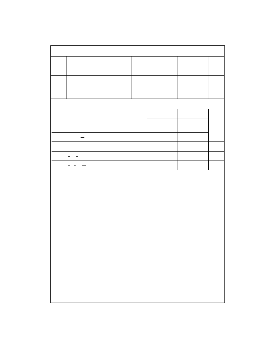
AC Electrical Characteristics
AC Operating Requirements
Symbol
Parameter
T
A
=
+
25
∞
C
T
A
=
0
∞
C to
+
70
∞
C
Units
V
CC
=
+
5.0V
V
CC
=
+
5.0V
C
L
=
50 pF
C
L
=
50 pF
Min
Typ
Max
Min
Max
f
MAX
Maximum Clock Frequency
85
105
80
MHz
t
PLH
Propagation Delay
2.0
5.0
6.5
2.0
7.5
ns
t
PHL
CP
n
to Q
n
or Q
n
2.0
5.0
6.5
2.0
7.5
t
PLH
Propagation Delay
2.0
4.5
6.5
2.0
7.5
ns
t
PHL
C
Dn
, S
Dn
to Q
n
, Q
n
2.0
4.5
6.5
2.0
7.5
Symbol
Parameter
T
A
=
+
25
∞
C
T
A
=
0
∞
C to
+
70
∞
C
Units
V
CC
=
+
5.0V
V
CC
=
+
5.0V
Min
Max
Min
Max
t
S
(H)
Setup Time, HIGH or LOW
4.0
5.0
ns
t
S
(L)
J
n
or K
n
to CP
n
3.0
3.5
t
H
(H)
Hold Time, HIGH or LOW
0
0
t
H
(L)
J
n
or K
n
to CP
n
0
0
t
W
(H)
CP Pulse Width
4.5
5.0
ns
t
W
(L)
HIGH or LOW
4.5
5.0
t
W
(L)
Pulse Width, LOW
4.5
5.0
ns
C
Dn
or S
Dn
t
REC
Recovery Time
4.0
5.0
ns
S
Dn
, C
Dn
to CP
5
www.fairchildsemi.com
74
F
1
12
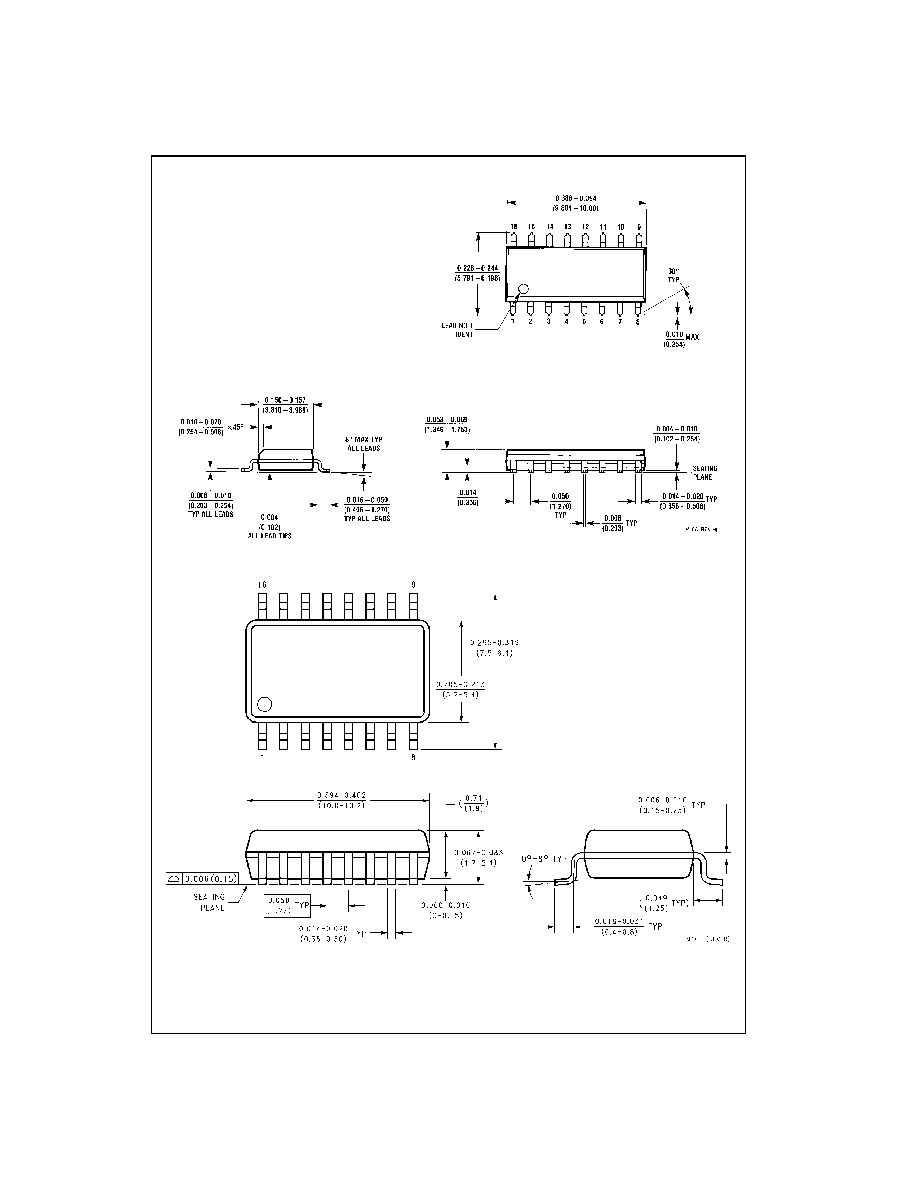
Physical Dimensions
inches (millimeters) unless otherwise noted
16-Lead Small Outline Integrated Circuit (SOIC), JEDEC MS-012, 0.150 Narrow
Package Number M16A
16-Lead Small Outline Package (SOP), EIAJ TYPE II, 5.3mm Wide
Package Number M16D
www.fairchildsemi.com
6
7
4
F1
1
2
Dua
l
J
K
Ne
ga
t
i
v
e
E
dge
-
T
r
igge
re
d Flip-
Flop
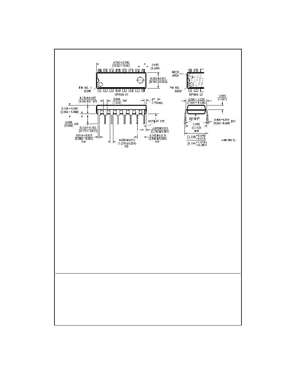
Physical Dimensions
inches (millimeters) unless otherwise noted (Continued)
16-Lead Plastic Dual-In-Line Package (PDIP), JEDEC MS-001, 0.300 Wide
Package Number N16E
Fairchild does not assume any responsibility for use of any circuitry described, no circuit patent licenses are implied and
Fairchild reserves the right at any time without notice to change said circuitry and specifications.
LIFE SUPPORT POLICY
FAIRCHILD'S PRODUCTS ARE NOT AUTHORIZED FOR USE AS CRITICAL COMPONENTS IN LIFE SUPPORT
DEVICES OR SYSTEMS WITHOUT THE EXPRESS WRITTEN APPROVAL OF THE PRESIDENT OF FAIRCHILD
SEMICONDUCTOR CORPORATION. As used herein:
1. Life support devices or systems are devices or systems
which, (a) are intended for surgical implant into the
body, or (b) support or sustain life, and (c) whose failure
to perform when properly used in accordance with
instructions for use provided in the labeling, can be rea-
sonably expected to result in a significant injury to the
user.
2. A critical component in any component of a life support
device or system whose failure to perform can be rea-
sonably expected to cause the failure of the life support
device or system, or to affect its safety or effectiveness.
www.fairchildsemi.com