 | –≠–ª–µ–∫—Ç—Ä–æ–Ω–Ω—ã–π –∫–æ–º–ø–æ–Ω–µ–Ω—Ç: 74F132SJ | –°–∫–∞—á–∞—Ç—å:  PDF PDF  ZIP ZIP |
© 1999 Fairchild Semiconductor Corporation
DS009477
www.fairchildsemi.com
April 1988
Revised July 1999
7
4F132 Q
uad 2-
Input
NAND S
c
hm
i
t
t
T
r
igg
e
r
74F132
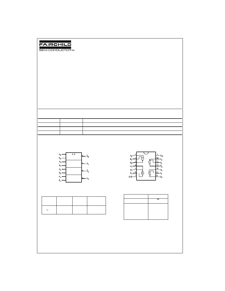
Quad 2-Input NAND Schmitt Trigger
General Description
The F132 contains four 2-input NAND gates which accept
standard TTL input signals and provide standard TTL out-
put levels. They are capable of transforming slowly chang-
ing input signals into sharply defined, jitter-free output
signals. In addition, they have a greater noise margin than
conventional NAND gates.
Each circuit contains a 2-input Schmitt Trigger followed by
level shifting circuitry and a standard FAST
TM
output struc-
ture. The Schmitt Trigger uses positive feedback to effec-
tively speed-up slow input transitions, and provide different
input threshold voltages for positive and negative-going
transitions. This hysteresis between the positive-going and
negative-going input threshold (typically 800 mV) is deter-
mined by resistor ratios and is essentially insensitive to
temperature and supply voltage variations.
Ordering Code:
Devices also available in Tape and Reel. Specify by appending the suffix letter "X" to the ordering code.
Logic Symbol
IEEE/IEC
Unit Loading/Fan Out
Connection Diagram
Function Table
H
=
HIGH Voltage Level
L
=
LOW Voltage Level
FAST
Æ
is a registered trademark of Fairchild Semiconductor Corporation
Order Number
Package Number
Package Description
74F132SC
M14A
14-Lead Small Outline Integrated Circuit (SOIC), JEDEC MS-120, 0.150 Narrow
74F132SJ
M14D
14-Lead Small Outline Package (SOP), EIAJ TYPE II, 5.3mm Wide
74F132PC
N14A
14-Lead Plastic Dual-In-Line Package (PDIP), JEDEC MS-001, 0.300 Wide
Pin Names Description
U.L.
Input I
IH
/I
IL
HIGH/LOW Output I
OH
/I
OL
A
n
, B
n
Inputs
1.0/1.0
20
µ
A/
-
0.6 mA
O
n
Outputs
50/33.3
-
1 mA/20 mA
Inputs
Outputs
A
B
O
L
L
H
L
H
H
H
L
H
H
H
L
www.fairchildsemi.com
2
74F132
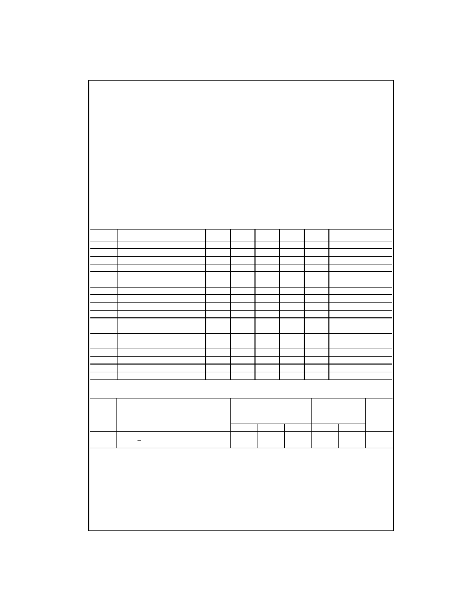
Absolute Maximum Ratings
(Note 1)
Recommended Operating
Conditions
Note 1: Absolute maximum ratings are values beyond which the device
may be damaged or have its useful life impaired. Functional operation
under these conditions is not implied.
Note 2: Either voltage limit or current limit is sufficient to protect inputs.
DC Electrical Characteristics
AC Electrical Characteristics
Storage Temperature
-
65
∞
C to
+
150
∞
C
Ambient Temperature under Bias
-
55
∞
C to
+
125
∞
C
Junction Temperature under Bias
-
55
∞
C to
+
150
∞
C
V
CC
Pin Potential to Ground Pin
-
0.5V to
+
7.0V
Input Voltage (Note 2)
-
0.5V to
+
7.0V
Input Current (Note 2)
-
30 mA to
+
5.0 mA
Voltage Applied to Output
in HIGH State (with V
CC
=
0V)
Standard Output
-
0.5V to V
CC
3-STATE Output
-
0.5V to
+
5.5V
Current Applied to Output
in LOW State (Max)
twice the rated I
OL
(mA)
ESD Last Passing Voltage (Min)
4000V
Free Air Ambient Temperature
0
∞
C to
+
70
∞
C
Supply Voltage
+
4.5V to
+
5.5V
Symbol
Parameter
Min
Typ
Max
Units
V
CC
Conditions
V
T
+
Positive-going Threshold
1.5
2.0
V
5.0
V
T
-
Negative-going Threshold
0.7
1.1
V
5.0
V
T
Hysteresis (V
T
+
-
V
T
-
)
0.4
V
5.0
V
CD
Input Clamp Diode Voltage
-
1.2
V
Min
I
IN
=
-
18 mA
V
OH
Output HIGH
10% V
CC
2.5
V
Min
I
OH
=
-
1 mA
Voltage
5% V
CC
2.7
I
OH
=
-
1 mA
V
OL
Output LOW Voltage
10% V
CC
0.5
V
Min
I
OL
=
20 mA
I
IH
Input HIGH Current
5.0
µ
A
Max
V
IN
=
2.7V
I
BVI
Input HIGH Current Breakdown Test
7.0
µ
A
Max
V
IN
=
7.0V
I
CEX
Output HIGH Leakage Current
50
µ
A
Max
V
OUT
=
V
CC
V
ID
Input Leakage Test
4.75
V
0.0
I
ID
=
1.9
µ
A
All Other Pins Grounded
I
OD
Output Leakage Circuit Current
3.75
µ
A
0.0
V
IOD
=
150 mV
All Other Pins Grounded
I
IL
Input LOW Current
-
0.6
mA
Max
V
IN
=
0.5V
I
OS
Output Short-Circuit Current
-
60
-
150
mA
Max
V
OUT
=
0V
I
CCH
Power Supply Current
17.0
mA
Max
V
O
=
HIGH
I
CCL
Power Supply Current
18.0
mA
Max
V
O
=
LOW
Symbol
Parameter
T
A
=
+
25
∞
C
T
A
=
0
∞
C to
+
70
∞
C
Units
V
CC
=
+
5.0V
V
CC
=
+
5.0V
C
L
=
50 pF
C
L
=
50 pF
Min
Typ
Max
Min
Max
t
PLH
Propagation Delay
4.0
10.5
3.5
12.0
ns
t
PHL
A
n
, B
n
to O
n
5.0
12.5
5.0
13.0

3
www.fairchildsemi.com
7
4F132
Physical Dimensions
inches (millimeters) unless otherwise noted
14-Lead Small Outline Integrated Circuit (SOIC), JEDEC MS-120, 0.150 Narrow
Package Number M14A
14-Lead Small Outline Package (SOP), EIAJ TYPE II, 5.3mm Wide
Package Number M14D

www.fairchildsemi.com
4
74F132
Quad 2-I
nput NAND
Schmit
t T
r
i
gger
Physical Dimensions
inches (millimeters) unless otherwise noted (Continued)
14-Lead Plastic Dual-In-Line Package (PDIP), JEDEC MS-001, 0.300 Wide
Package Number N14A
Fairchild does not assume any responsibility for use of any circuitry described, no circuit patent licenses are implied and
Fairchild reserves the right at any time without notice to change said circuitry and specifications.
LIFE SUPPORT POLICY
FAIRCHILD'S PRODUCTS ARE NOT AUTHORIZED FOR USE AS CRITICAL COMPONENTS IN LIFE SUPPORT
DEVICES OR SYSTEMS WITHOUT THE EXPRESS WRITTEN APPROVAL OF THE PRESIDENT OF FAIRCHILD
SEMICONDUCTOR CORPORATION. As used herein:
1. Life support devices or systems are devices or systems
which, (a) are intended for surgical implant into the
body, or (b) support or sustain life, and (c) whose failure
to perform when properly used in accordance with
instructions for use provided in the labeling, can be rea-
sonably expected to result in a significant injury to the
user.
2. A critical component in any component of a life support
device or system whose failure to perform can be rea-
sonably expected to cause the failure of the life support
device or system, or to affect its safety or effectiveness.
www.fairchildsemi.com