 | –≠–ª–µ–∫—Ç—Ä–æ–Ω–Ω—ã–π –∫–æ–º–ø–æ–Ω–µ–Ω—Ç: 74F151ACW | –°–∫–∞—á–∞—Ç—å:  PDF PDF  ZIP ZIP |
© 2000 Fairchild Semiconductor Corporation
DS009481
www.fairchildsemi.com
April 1988
Revised September 2000
7
4
F151A 8
-
I
nput
Mult
ipl
exer
74F151A
8-Input Multiplexer
General Description
The F151A is a high-speed 8-input digital multiplexer. It
provides in one package the ability to select one line of
data from up to eight sources. The F151A can be used as a
universal function generator to generate any logic function
of four variables. Both assertion and negation outputs are
provided.
Ordering Code:
Devices also available in Tape and Reel. Specify by appending the suffix letter "X" to the ordering code.
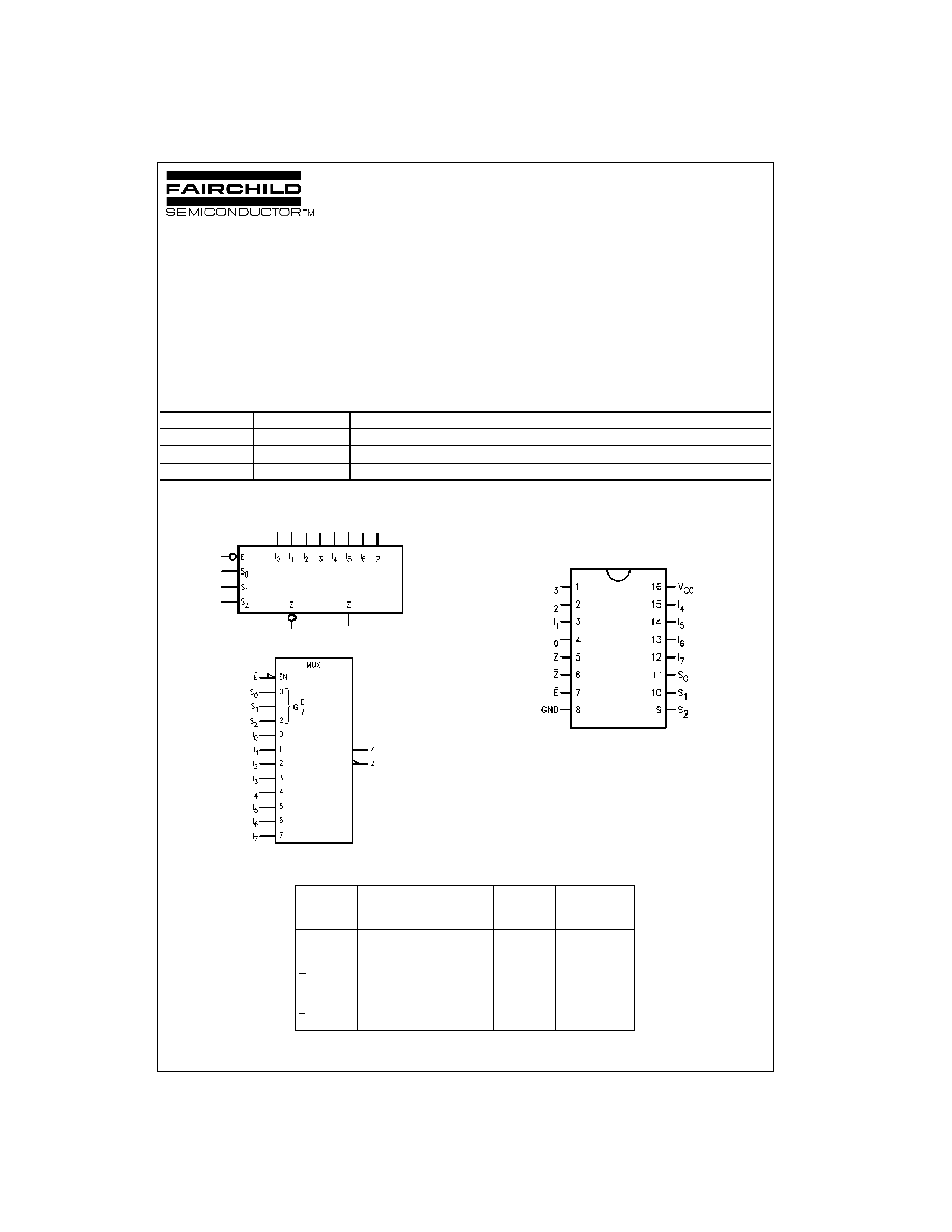
Logic Symbols
IEEE/IEC
Connection Diagram
Unit Loading/Fan Out
Order Number
Package Number
Package Description
74F151ASC
M16A
16-Lead Small Outline Integrated Circuit (SOIC), JEDEC MS-012, 0.150 Narrow
74F151ASJ
M16D
16-Lead Small Outline Package (SOP), EIAJ TYPE II, 5.3mm Wide
74F151APC
N16E
16-Lead Plastic Dual-In-Line Package (PDIP), JEDEC MS-001, 0.300 Wide
Pin Names
Description
U.L.
Input I
IH
/I
IL
HIGH/LOW Output I
OH
/I
OL
I
0
≠I
7
Data Inputs
1.0/1.0
20
µ
A/
-
0.6 mA
S
0
≠S
2
Select Inputs
1.0/1.0
20
µ
A/
-
0.6 mA
E
Enable Input (Active LOW)
1.0/1.0
20
µ
A/
-
0.6 mA
Z
Data Output
50/33.3
-
1 mA/20 mA
Z
Inverted Data Output
50/33.3
-
1 mA/20 mA
www.fairchildsemi.com
2
74F15
1A
Functional Description
The F151A is a logic implementation of a single pole, 8-
position switch with the switch position controlled by the
state of three Select inputs, S
0
, S
1
, S
2
. Both assertion and
negation outputs are provided. The Enable input (E) is
active LOW. When it is not activated, the negation output is
HIGH and the assertion output is LOW regardless of all
other inputs. The logic function provided at the output is:
Z
=
E ∑ (I
0
S
2
S
1
S
0
+
I
1
S
2
S
1
S
0
+
I
2
S
2
S
1
S
0
+
I
3
S
2
S
1
S
0
+
I
4
S
2
S
1
S
0
+
I
5
S
2
S
1
S
0
+
I
6
S
2
S
1
S
0
+
I
7
S
2
S
1
S
0
)
The F151A provides the ability, in one package, to select
from eight sources of data or control information. By proper
manipulation of the inputs, the F151A can provide any logic
function of four variables and its negation.
Truth Table
H
=
HIGH Voltage Level
L
=
LOW Voltage Level
X
=
Immaterial
Logic Diagram
Please note that this diagram is provided only for the understanding of logic operations and should not be used to estimate propagation delays.
Inputs
Outputs
E
S
2
S
1
S
0
Z
Z
H
X
X
X
H
L
L
L
L
L
I
0
I
0
L
L
L
H
I
1
I
1
L
L
H
L
I
2
I
2
L
L
H
H
I
3
I
3
L
H
L
L
I
4
I
4
L
H
L
H
I
5
I
5
L
H
H
L
I
6
I
6
L
H
H
H
I
7
I
7
3
www.fairchildsemi.com
7
4
F151A
Absolute Maximum Ratings
(Note 1)
Recommended Operating
Conditions
Note 1: Absolute maximum ratings are values beyond which the device
may be damaged or have its useful life impaired. Functional operation
under these conditions is not implied.
Note 2: Either voltage limit or current limit is sufficient to protect inputs.
DC Electrical Characteristics
Storage Temperature
-
65
∞
C to
+
150
∞
C
Ambient Temperature under Bias
-
55
∞
C to
+
125
∞
C
Junction Temperature under Bias
-
55
∞
C to
+
150
∞
C
V
CC
Pin Potential to
Ground Pin
-
0.5V to
+
7.0V
Input Voltage (Note 2)
-
0.5V to
+
7.0V
Input Current (Note 2)
-
30 mA to
+
5.0 mA
Voltage Applied to Output
in HIGH State (with V
CC
=
0V)
Standard Output
-
0.5V to V
CC
3-STATE Output
-
0.5V to
+
5.5V
Current Applied to Output
in LOW State (Max)
twice the rated I
OL
(mA)
Free Air Ambient Temperature
0
∞
C to
+
70
∞
C
Supply Voltage
+
4.5V to
+
5.5V
Symbol
Parameter
Min
Typ
Max
Units
V
CC
Conditions
V
IH
Input HIGH Voltage
2.0
V
Recognized as a HIGH Signal
V
IL
Input LOW Voltage
0.8
V
Recognized as a LOW Signal
V
CD
Input Clamp Diode Voltage
-
1.2
V
Min
I
IN
=
-
18 mA
V
OH
Output HIGH
10% V
CC
2.5
V
Min
I
OH
=
-
1 mA
Voltage
5% V
CC
2.7
I
OH
=
-
1 mA
V
OL
Output LOW Voltage
10% V
CC
0.5
V
Min
I
OL
=
20 mA
I
IH
Input HIGH Current
5.0
µ
A
Max
V
IN
=
2.7V
I
BVI
Input HIGH Current
7.0
µ
A
Max
V
IN
=
7.0V
Breakdown Test
I
CEX
Output HIGH
50
µ
A
Max
V
OUT
=
V
CC
Leakage Current
V
ID
Input Leakage
4.75
V
0.0
I
ID
=
1.9
µ
A
Test
All Other Pins Grounded
I
OD
Output Leakage
3.75
µ
A
0.0
V
IOD
=
150 mV
Circuit Current
All Other Pins Grounded
I
IL
Input LOW Current
-
0.6
mA
Max
V
IN
=
0.5V
I
OS
Output Short-Circuit Current
-
60
-
150
mA
Max
V
OUT
=
0V
I
CC
Power Supply Current
13.5
21.0
mA
Max
V
O
=
HIGH
www.fairchildsemi.com
4
74F15
1A
AC Electrical Characteristics
Symbol
Parameter
T
A
=
+
25
∞
C
T
A
=
0
∞
C to
+
70
∞
C
Units
V
CC
=
+
5.0V
C
L
=
50 pF
C
L
=
50 pF
Min
Typ
Max
Min
Max
t
PLH
Propagation Delay
4.0
6.2
9.0
3.5
9.5
ns
t
PHL
S
n
to Z
3.2
5.2
7.5
3.2
7.5
t
PLH
Propagation Delay
4.5
7.5
10.5
4.5
12.0
ns
t
PHL
S
n
to Z
4.0
6.2
9.0
4.0
9.0
t
PLH
Propagation Delay
3.0
4.7
6.1
3.0
7.0
ns
t
PHL
E to Z
3.0
4.4
6.0
2.5
6.0
t
PLH
Propagation Delay
5.0
7.0
9.5
4.0
10.5
ns
t
PHL
E to Z
3.5
5.3
7.0
3.0
7.5
t
PLH
Propagation Delay
3.0
4.8
6.5
3.0
7.0
ns
t
PHL
I
n
to Z
1.5
2.5
4.0
1.5
5.0
t
PLH
Propagation Delay
3.0
4.8
6.5
2.5
7.5
ns
t
PHL
I
n
to Z
3.7
5.5
7.0
3.7
7.5
5
www.fairchildsemi.com
7
4
F151A
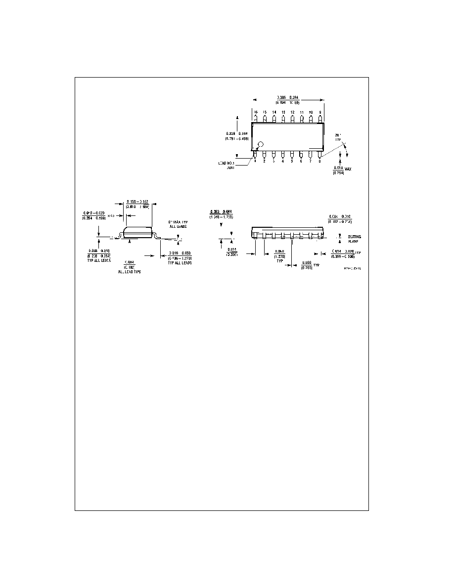
Physical Dimensions
inches (millimeters) unless otherwise noted
16-Lead Small Outline Integrated Circuit (SOIC), JEDEC MS-012, 0.150 Narrow
Package Number M16A