© 1999 Fairchild Semiconductor Corporation
DS009491
www.fairchildsemi.com
April 1988
Revised July 1999
7
4F181 4-Bi
t Arit
hmeti
c
Lo
gic Unit
74F181
4-Bit Arithmetic Logic Unit
General Description
The 74F181 is a 4-bit Arithmetic logic Unit (ALU) which can
perform all the possible 16 logic operations on two vari-
ables and a variety of arithmetic operations. It is 40% faster
than the Schottky ALU and only consumes 30% as much
power.
Features
s
Full lookahead for high-speed arithmetic operation on
long words
Ordering Code:
Devices also available in Tape and Reel. Specify by appending the suffix letter "X" to the ordering code.
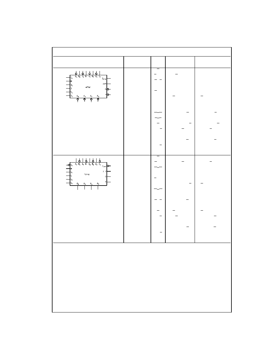
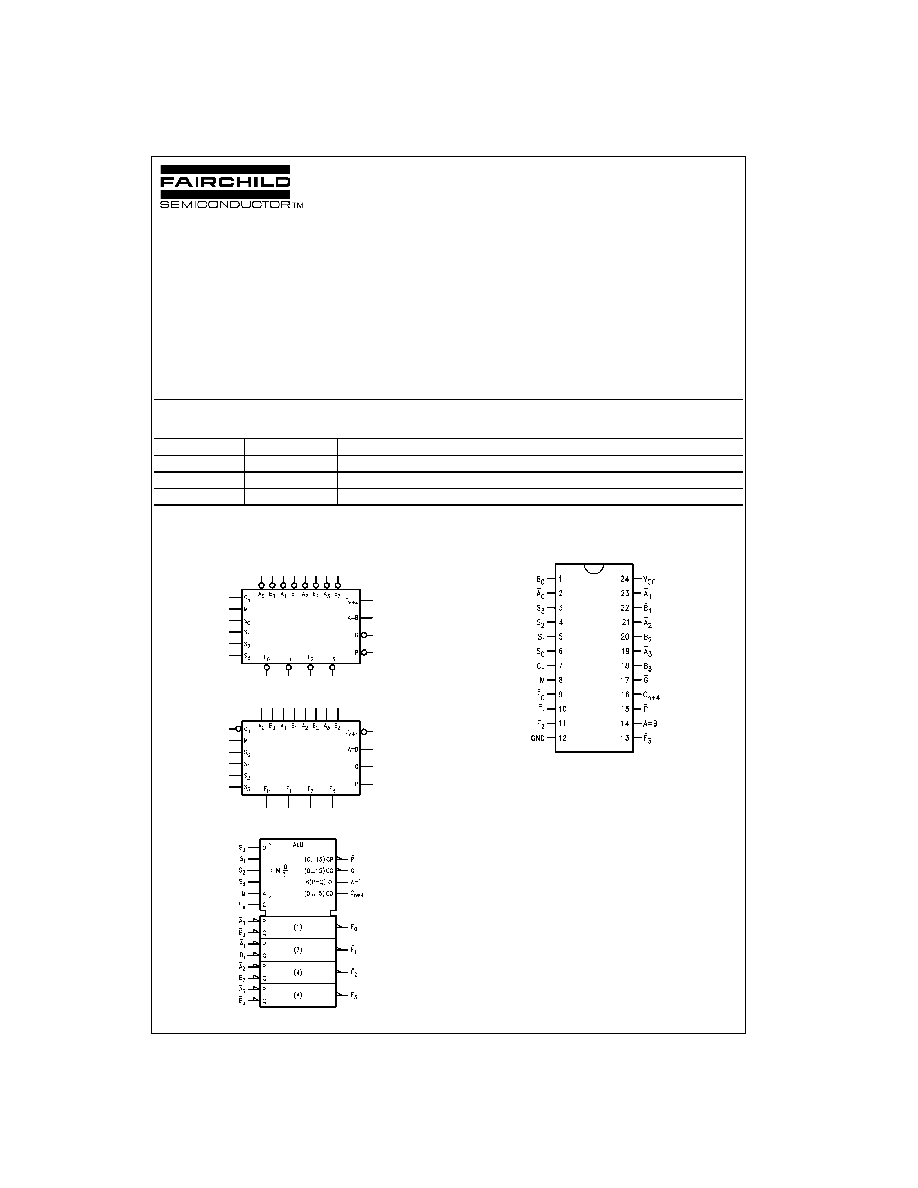
Logic Symbols
Active-HIGH Operands
Active-LOW Operands
IEEE/IEC
Connection Diagram
Order Number
Package Number
Package Description
74F181SC
M24B
24-Lead Small Outline Integrated Circuit (SOIC), JEDEC MS-013, 0.300 Wide
74F181PC
N24A
24-Lead Plastic Dual-In-Line Package (PDIP), JEDEC MS-010, 0.600 Wide
74F181SPC
N24C
24-Lead Plastic Dual-In-Line Package (PDIP), JEDEC MS-100, 0.300 Wide

www.fairchildsemi.com
2
74F181
Unit Loading/Fan Out
Note 1: OC-Open Collector
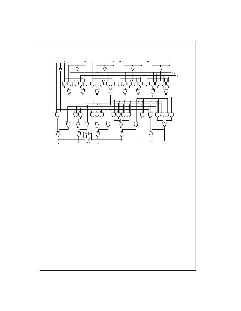
Functional Description
The 74F181 is a 4-bit high-speed parallel Arithmetic Logic
Unit (ALU). Controlled by the four Function Select inputs
(S
0
≠S
3
) and the Mode Control input (M), it can perform all
the 16 possible logic operations or 16 different arithmetic
operations on Active HIGH or Active LOW operands. The
Function Table lists these operations.
When the Mode Control input (M) is HIGH, all internal car-
ries are inhibited and the device performs logic operations
on the individual bits as listed. When the Mode Control
input is LOW, the carries are enabled and the device per-
forms arithmetic operations on the two 4-bit words. The
device incorporates full internal carry lookahead and pro-
vides for either ripple carry between devices using the
C
n
+
4
output, or for carry lookahead between packages
using the signals P (Carry Propagate) and G (Carry Gener-
ate). In the Add mode, P indicates that F is 15 or more,
while G indicates that F is 16 or more. In the Subtract mode
P indicates that F is zero or less, while G indicates that F is
less than zero. P and G are not affected by carry in. When
speed requirements are not stringent, the 74F181 can be
used in a simple Ripple Carry mode by connecting the
Carry output (C
n
+
4) signal to the Carry input (C
n
) of the
next unit. For high speed operation the device is used in
conjunction with a carry lookahead circuit. One carry looka-
head package is required for each group of four 74F181
devices. Carry lookahead can be provided at various levels
and offers high speed capability over extremely long word
lengths.
The A
=
B output from the device goes HIGH when all four
F outputs are HIGH and can be used to indicate logic
equivalence over four bits when the unit is in the Subtract
mode. The A
=
B output is open collector and can be wired
AND with other A
=
B outputs to give a comparison for
more than four bits. The A
=
B signal can also be used with
the C
n
+
4
signal to indicate A
>
B and A
<
B.
The Function Table lists the arithmetic operations that are
performed without a carry in. An incoming carry adds a one
to each operation. Thus, select code LHHL generates A
minus B minus 1 (2s complement notation) without a carry
in and generates A minus B when a carry is applied.
Because subtraction is actually performed by complemen-
tary addition (1s complement), a carry out means borrow;
thus a carry is generated when there is no underflow and
no carry is generated when there is underflow. As indi-
cated, this device can be used with either active LOW
inputs producing active LOW outputs or with active HIGH
inputs producing active HIGH outputs. For either case the
table lists the operations that are performed to the oper-
ands labeled inside the logic symbol.
Pin Names
Description
U.L.
Input I
IH
/I
IL
HIGH/LOW
Output I
OH
/I
OL
A
0
≠A
3
A Operand Inputs (Active LOW)
1.0/3.0
20
µ
A/
-
1.8 mA
B
0
≠B
3
B Operand Inputs (Active LOW)
1.0/3.0
20
µ
A/
-
1.8 mA
S
0
≠S
3
Function Select Inputs
1.0/4.0
20
µ
A/
-
2.4 mA
M
Mode Control Input
1.0/1.0
20
µ
A/
-
0.6 mA
C
n
Carry Input
1.0/5.0
20
µ
A/
-
3.0 mA
F
0
≠F
3
Function Outputs (Active LOW)
50/33.3
-
1 mA/20 mA
A
=
B
Comparator Output
OC (Note 1)/33.3
(Note 1)/20 mA
G
Carry Generate Output (Active LOW)
50/33.3
-
1 mA/20 mA
P
Carry Propagate Output (Active LOW)
50/33.3
-
1 mA/20 mA
C
n
+
4
Carry Output
50/33.3
-
1 mA/20 mA