 | –≠–ª–µ–∫—Ç—Ä–æ–Ω–Ω—ã–π –∫–æ–º–ø–æ–Ω–µ–Ω—Ç: 74F189SJ | –°–∫–∞—á–∞—Ç—å:  PDF PDF  ZIP ZIP |
© 1999 Fairchild Semiconductor Corporation
DS009493
www.fairchildsemi.com
April 1988
Revised July 1999
7
4F189 64-Bi
t Random
Access Mem
o
r
y
wi
th 3-
S
T
A
T
E
Out
puts
74F189
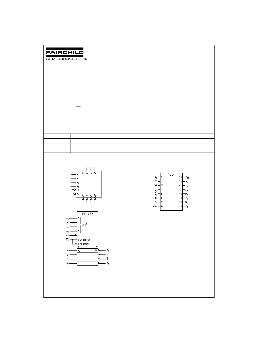
64-Bit Random Access Memory with 3-STATE Outputs
General Description
The F189 is a high-speed 64-bit RAM organized as a 16-
word by 4-bit array. Address inputs are buffered to mini-
mize loading and are fully decoded on-chip. The outputs
are 3-STATE and are in the high impedance state when-
ever the Chip Select (CS) input is HIGH. The outputs are
active only in the Read mode and the output data is the
complement of the stored data.
Features
s
3-STATE outputs for data bus applications
s
Buffered inputs minimize loading
s
Address decoding on-chip
s
Diode clamped inputs minimize ringing
Ordering Code:
Devices also available in Tape and Reel. Specify by appending suffix "X" to the ordering code.
Logic Symbols
IEEE/IEC
Connection Diagram
Order Number
Package Number
Package Description
74F189SC M16B
16-Lead Small Outline Integrated Circuit (SOIC), JEDEC MS-013, 0.300" Wide
74F189SJ
M16D
16-Lead Small Outline Package (SOP), EIAJ TYPE II, 5.3mm Wide
74F189PC
N16E
16-Lead Plastic Dual-In-Line Package (PDIP), JEDEC MS-001, 0.300" Wide

www.fairchildsemi.com
2
74F189
Unit Loading/Fan Out
Function Table
H
=
HIGH Voltage Level
L
=
LOW Voltage Level
X
=
Immaterial
Block Diagram
Pin Names
Description
U.L.
Input I
IH
/I
IL
HIGH/LOW
Output I
OH
/I
OL
A
0
≠A
3
Address Inputs
1.0/1.0
20
µ
A/
-
0.6 mA
CS
Chip Select Input (Active LOW)
1.0/1.0
20
µ
A/
-
1.2 mA
WE
Write Enable Input (Active LOW)
1.0/1.0
20
µ
A/
-
0.6 mA
D
0
≠D
3
Data Inputs
1.0/1.0
20
µ
A/
-
0.6 mA
O
0
≠O
3
Inverted Data Outputs
150/40 (33.3)
-
3.0 mA/24 mA (20 mA)
Inputs
Operation
Condition of Outputs
CS
WE
L
L
Write
High Impedance
L
H
Read
Complement of Stored Data
H
X
Inhibit
High Impedance

3
www.fairchildsemi.com
7
4F189
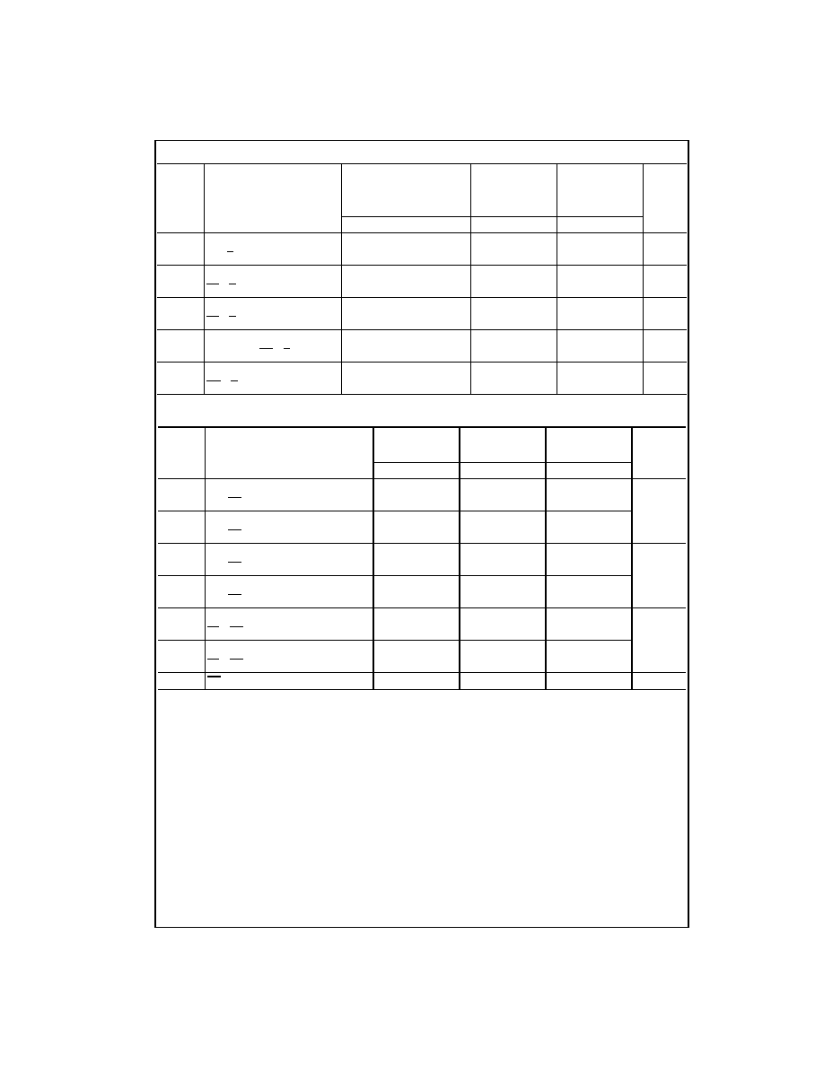
Absolute Maximum Ratings
(Note 1)
Recommended Operating
Conditions
Note 1: Absolute maximum ratings are values beyond which the device
may be damaged or have its useful life impaired. Functional operation
under these conditions is not implied.
Note 2: Either voltage limit or current limit is sufficient to protect inputs.
DC Electrical Characteristics
Storage Temperature
-
65
∞
C to
+
150
∞
C
Ambient Temperature under Bias
-
55
∞
C to
+
125
∞
C
Junction Temperature under Bias
-
55
∞
C to
+
175
∞
C
V
CC
Pin Potential to
Ground Pin
-
0.5V to
+
7.0V
Input Voltage (Note 2)
-
0.5V to
+
7.0V
Input Current (Note 2)
-
30 mA to
+
5.0 mA
Voltage Applied to Output
in HIGH State (with V
CC
=
0V)
Standard Output
-
0.5V to V
CC
3-STATE Output
-
0.5V to
+
5.5V
Current Applied to Output
in LOW State (Max)
Free Air Ambient Temperature
0
∞
C to
+
70
∞
C
Supply Voltage
+
4.5V to
+
5.5V
Symbol
Parameter
Min
Typ
Max
Units
V
CC
Conditions
V
IH
Input HIGH Voltage
2.0
V
Recognized as a HIGH Signal
V
IL
Input LOW Voltage
0.8
V
Recognized as a LOW Signal
V
CD
Input Clamp Diode Voltage
-
1.2
V
Min
I
IN
=
-
18 mA
V
OH
Output HIGH
10% V
CC
2.5
V
Min
I
OH
=
-
1 mA
Voltage
10% V
CC
2.4
I
OH
=
-
3 mA
5% V
CC
2.7
I
OH
=
-
1 mA
5% V
CC
2.7
I
OH
=
-
3 mA
V
OL
Output LOW
Voltage
10% V
CC
0.5
V
Min
I
OL
=
24 mA
I
IH
Input HIGH
Current
5.0
µ
A
Max
V
IN
= 2.7V
I
BVI
Input HIGH Current
Breakdown Test
7.0
µ
A
Max
V
IN
=
7.0V
I
CEX
Output HIGH
Leakage Current
50
µ
A
Max
V
OUT
=
V
CC
V
ID
Input Leakage
4.75
V
0.0
I
ID
=
1.9
µ
A
Test
All Other Pins Grounded
I
OD
Output Leakage
3.75
µ
A
0.0
V
IOD
=
150 mV
Circuit Current
All Other Pins Grounded
I
IL
Input LOW Current
-
0.6
mA
Max
V
IN
=
0.5V (except CS)
-
1.2
V
IN
=
0.5V (CS)
I
OZH
Output Leakage Current
50
µ
A
Max
V
OUT
=
2.7V
I
OZL
Output Leakage Current
-
50
µ
A
Max
V
OUT
=
0.5V
I
OS
Output Short-Circuit Current
-
60
-
150
mA
Max
V
OUT
=
0V
I
ZZ
Bus Drainage Test
500
µ
A
0.0V
V
OUT
=
5.25V
I
CCZ
Power Supply Current
37
55
mA
Max
V
O
=
HIGH Z
www.fairchildsemi.com
4
74F189
AC Electrical Characteristics
AC Operating Requirements
Symbol
Parameter
T
A
=
+
25
∞
C
T
A
=
-
55
∞
C to
+
125
∞
C
T
A
=
0
∞
C to
+
70
∞
C
Units
V
CC
=
+
5.0V
V
CC
=
+
5.0V
V
CC
=
+
5.0V
C
L
=
50 pF
C
L
=
50 pF
C
L
=
50 pF
Min
Typ
Max
Min
Max
Min
Max
t
PLH
Access Time, HIGH or LOW
10.0
18.5
26.0
9.0
32.0
10.0
27.0
ns
t
PHL
A
n
to O
n
8.0
13.5
19.0
8.0
23.0
8.0
20.0
t
PZH
Access Time, HIGH or LOW
3.5
6.0
8.5
3.5
10.5
3.5
9.5
ns
t
PZL
CS to O
n
5.0
9.0
13.0
5.0
15.0
5.0
14.0
t
PHZ
Disable Time, HIGH or LOW
2.0
4.0
6.0
2.0
8.0
2.0
7.0
ns
t
PLZ
CS to O
n
3.0
5.5
8.0
2.5
10.0
3.0
9.0
t
PZH
Write Recovery Time,
6.5
15.0
28.0
6.5
37.5
6.5
29.0
ns
t
PZL
HIGH or LOW WE to O
n
6.5
11.0
15.5
6.5
17.5
6.5
16.5
t
PHZ
Disable Time, HIGH or LOW
4.0
7.0
10.0
3.5
12.0
4.0
11.0
ns
t
PLZ
WE to O
n
5.0
9.0
13.0
5.0
15.0
5.0
14.0
Symbol
Parameter
T
A
=
+
25
∞
C
T
A
=
-
55
∞
C to
+
125
∞
C
T
A
=
0
∞
C to
+
70
∞
C
Units
V
CC
=
+
5.0V
V
CC
=
+
5.0V
V
CC
=
+
5.0V
Min
Max
Min
Max
Min
Max
t
S
(H)
Setup Time, HIGH or LOW
0
0
0
ns
t
S
(L)
A
n
to WE
0
0
0
t
H
(H)
Hold Time, HIGH or LOW
2.0
2.0
2.0
t
H
(L)
A
n
to WE
2.0
2.0
2.0
t
S
(H)
Setup Time, HIGH or LOW
10.0
11.0
10.0
ns
t
S
(L)
D
n
to WE
10.0
11.0
10.0
t
H
(H)
Hold Time, HIGH or LOW
0
2.0
0
t
H
(L)
D
n
to WE
0
2.0
0
t
S
(L)
Setup Time, LOW
0
0
0
ns
CS to WE
t
H
(L)
Hold Time, LOW
6.0
7.5
6.0
CS to WE
t
W
(L)
WE Pulse Width, LOW
6.0
15.0
6.0
ns

5
www.fairchildsemi.com
7
4F189
Physical Dimensions
inches (millimeters) unless otherwise noted
16-Lead Small Outline Integrated Circuit (SOIC), JEDEC MS013, 0.300" Wide Body
Package Number M16B
16-Lead Plastic Dual-In-Line Package (PDIP), JEDEC MS-OO1, 0.300" Wide
Package Number N16E