© 1999 Fairchild Semiconductor Corporation
DS009497
www.fairchildsemi.com
April 1988
Revised July 1999
7
4F193 U
p
/
D
own
Bi
nary Count
er w
i
th Separ
ate Up/Down Clocks
74F193
Up/Down Binary Counter with Separate Up/Down Clocks
General Description
The 74F193 is an up/down modulo-16 binary counter. Sep-
arate Count Up and Count Down Clocks are used, and in
either counting mode the circuits operate synchronously.
The outputs change state synchronously with the LOW-to-
HIGH transitions on the clock inputs. Separate Terminal
Count Up and Terminal Count Down outputs are provided
that are used as the clocks for subsequent stages without
extra logic, thus simplifying multi-stage counter designs.
Individual preset inputs allow the circuit to be used as a
programmable counter. Both the Parallel Load (PL) and the
Master Reset (MR) inputs asynchronously override the
clocks.
Ordering Code:
Devices also available in Tape and Reel. Specify by appending suffix letter "X" to the ordering code.
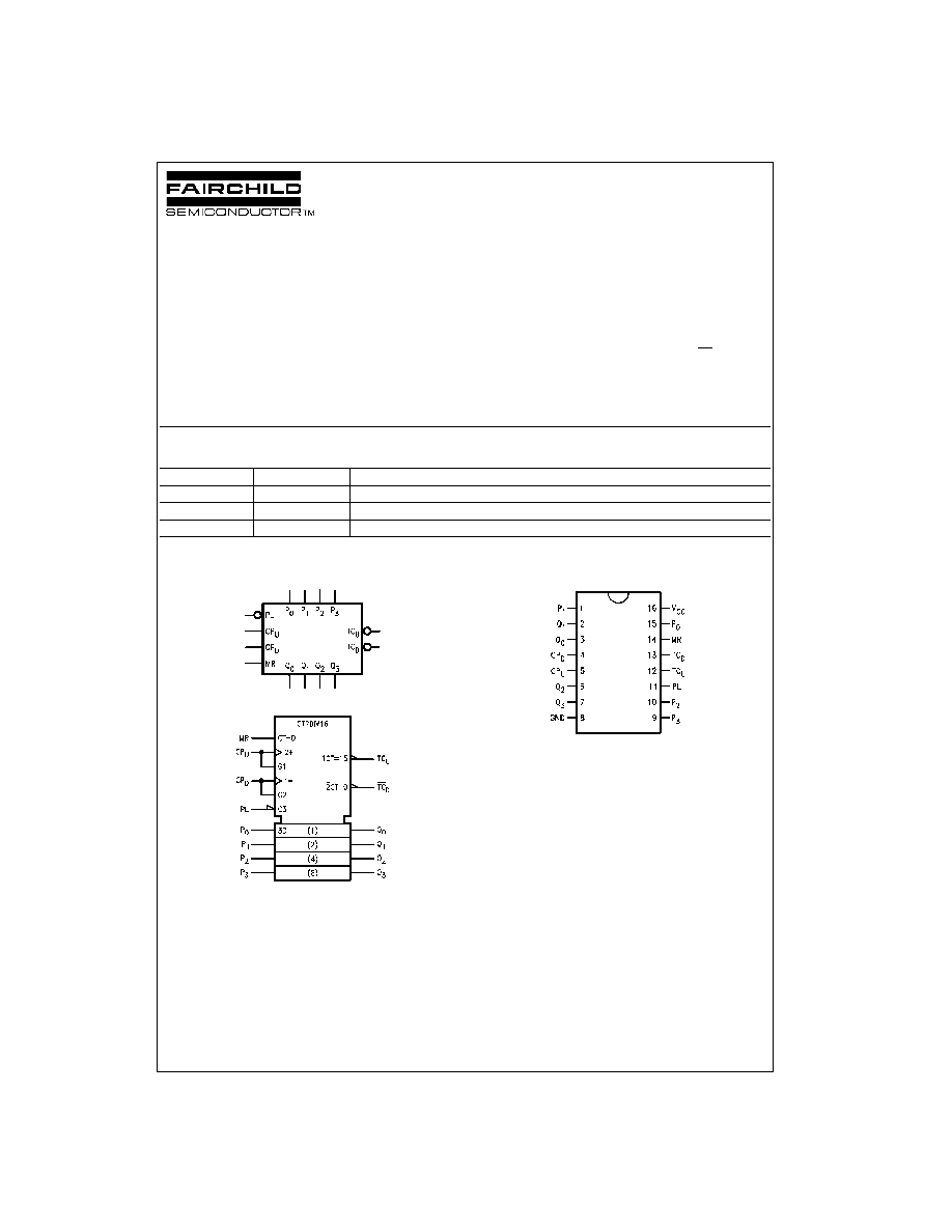
Logic Symbols
IEEE/IEC
Connection Diagram
Order Number
Package Number
Package Description
74F193SC M16A
16-Lead Small Outline Integrated Circuit (SOIC), JEDEC MS-012, 0.150" Narrow Body
74F193SJ
M16D
16-Lead Small Outline Package (SOP), EIAJ TYPE II, 5.3mm Wide
74F193PC
N16E
16-Lead Plastic Dual-In-Line Package (PDIP), JEDEC MS-001, 0.300" Wide
www.fairchildsemi.com
2
74F193
Unit Loading/Fan Out
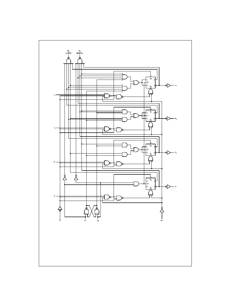
Functional Description
The 74F193 is a 4-bit binary synchronous up/down (revers-
ible) counter. It contains four edge-triggered flip-flops, with
internal gating and steering logic to provide master reset,
individual preset, count up and count down operations.
A LOW-to-HIGH transition on the CP input to each flip-flop
causes the output to change state. Synchronous switching,
as opposed to ripple counting, is achieved by driving the
steering gates of all stages from a common Count Up line
and a common Count Down line, thereby causing all state
changes to be initiated simultaneously. A LOW-to-HIGH
transition on the Count Up input will advance the count by
one; a similar transition on the Count Down input will
decrease the count by one. While counting with one clock
input, the other should be held HIGH, as indicated in the
Function Table.
The Terminal Count Up (TC
U
) and Terminal Count Down
(TC
D
) outputs are normally HIGH. When the circuit has
reached the maximum count state 15, the next HIGH-to-
LOW transition of the Count Up Clock will cause TC
U
to go
LOW. TC
U
will stay LOW until CP
U
goes HIGH again, thus
effectively repeating the Count Up Clock, but delayed by
two gate delays. Similarly, the TC
D
output will go LOW
when the circuit is in the zero state and the Count Down
Clock goes LOW. Since the TC outputs repeat the clock
waveforms, they can be used as the clock input signals to
the next higher order circuit in a multistage counter.
TC
U
=
Q
0
· Q
1
· Q
2
· Q
3
· CP
U
TC
D
=
Q
0
· Q
1
· Q
2
· Q
3
· CP
D
The 74F193 has an asynchronous parallel load capability
permitting the counter to be preset. When the Parallel Load
(PL) and the Master Reset (MR) inputs are LOW, informa-
tion present on the Parallel Data input (P
0
P
3
) is loaded
into the counter and appears on the outputs regardless of
the conditions of the clock inputs. A HIGH signal on the
Master Reset input will disable the preset gates, override
both clock inputs, and latch each Q output in the LOW
state. If one of the clock inputs is LOW during and after a
reset or load operation, the next LOW-to-HIGH transition of
that clock will be interpreted as a legitimate signal and will
be counted.
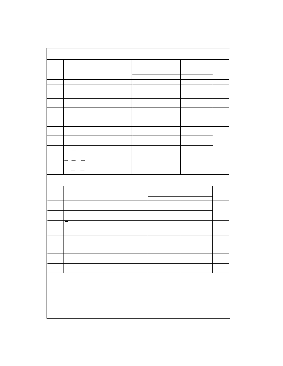
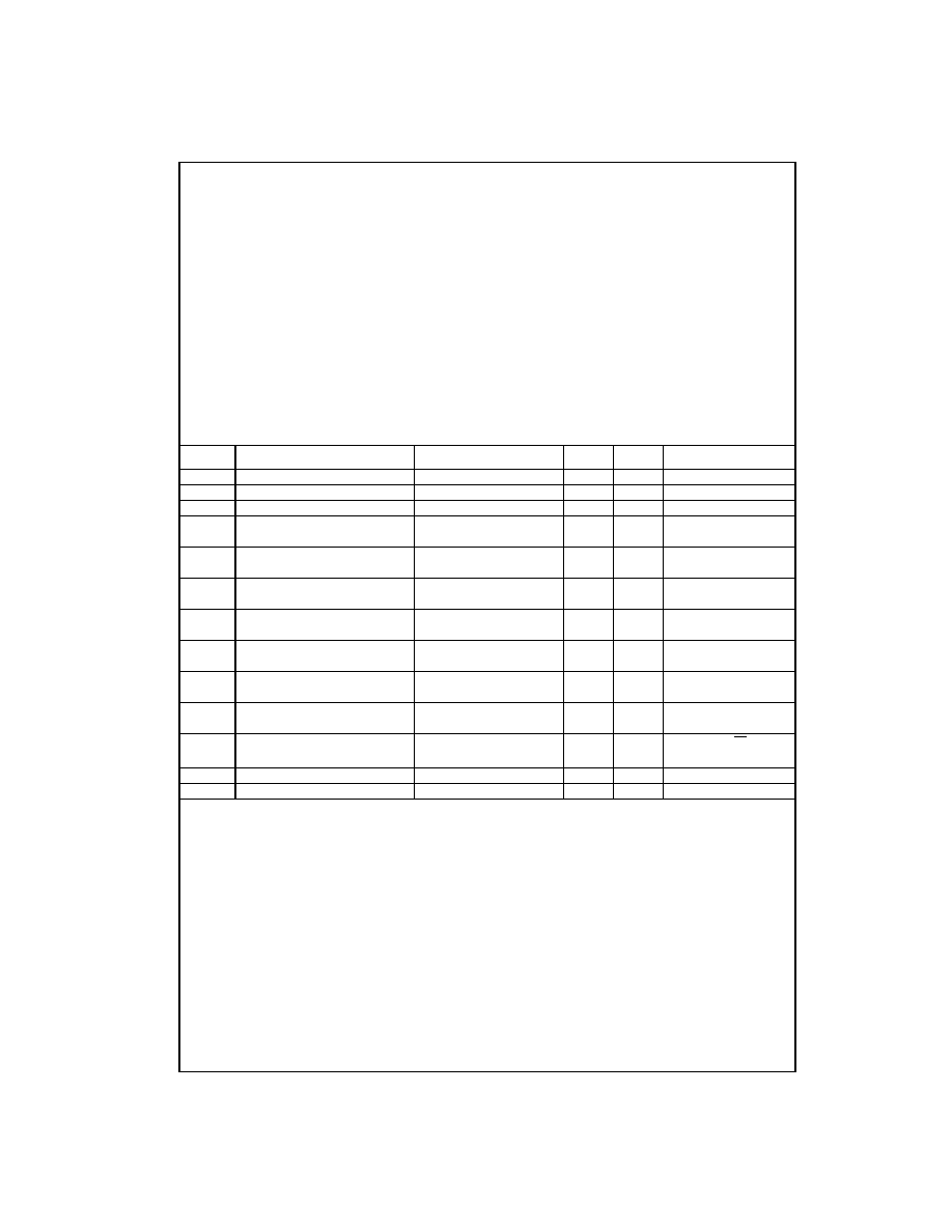
Function Table
H
=
HIGH Voltage Level
L
=
LOW Voltage Level
X
=
Immaterial
=
LOW-to-HIGH Clock Transition
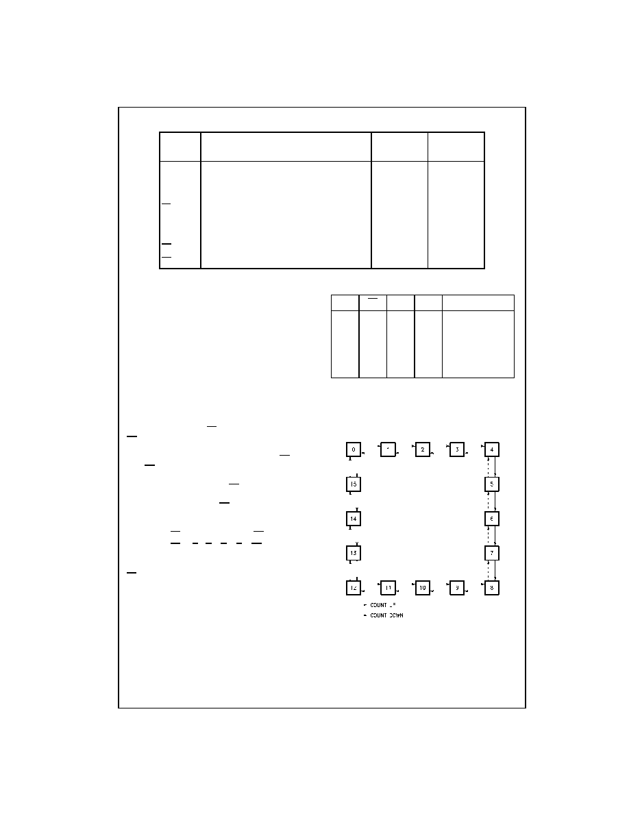
State Diagram
Pin Names
Description
U.L.
Input I
IH
/I
IL
HIGH/LOW
Output I
OH
/I
OL
CP
U
Count Up Clock Input (Active Rising Edge)
1.0/3.0
20
µ
A/
-
1.8 mA
CP
D
Count Down Clock Input (Active Rising Edge)
1.0/3.0
20
µ
A/
-
1.8 mA
MR
Asynchronous Master Reset Input (Active HIGH)
1.0/1.0
20
µ
A/
-
0.6 mA
PL
Asynchronous Parallel Load Input (Active LOW)
1.0/1.0
20
µ
A/
-
0.6 mA
P
0
P
3
Parallel Data Inputs
1.0/1.0
20
µ
A/
-
0.6 mA
Q
0
Q
3
Flip-Flop Outputs
50/33.3
-
1 mA/20 mA
TC
D
Terminal Count Down (Borrow) Output (Active LOW)
50/33.3
-
1 mA/20 mA
TC
U
Terminal Count Up (Carry) Output (Active LOW)
50/33.3
-
1 mA/20 mA
MR
PL
CP
U
CP
D
Mode
H
X
X
X
Reset (Asyn.)
L
L
X
X
Preset (Asyn.)
L
H
H
H
No Change
L
H
H
Count Up
L
H
H
Count Down
www.fairchildsemi.com
4
74F193
Absolute Maximum Ratings
(Note 1)
Recommended Operating
Conditions
Note 1: Absolute maximum ratings are values beyond which the device
may be damaged or have its useful life impaired. Functional operation
under these conditions is not implied.
Note 2: Either voltage limit or current limit is sufficient to protect inputs.
DC Electrical Characteristics
Storage Temperature
-
65
°
C to
+
150
°
C
Ambient Temperature under Bias
-
55
°
C to
+
125
°
C
Junction Temperature under Bias
-
55
°
C to
+
150
°
C
V
CC
Pin Potential to Ground Pin
-
0.5V to
+
7.0V
Input Voltage (Note 2)
-
0.5V to
+
7.0V
Input Current (Note 2)
-
30 mA to
+
5.0 mA
Voltage Applied to Output
in HIGH State (with V
CC
=
0V)
Standard Output
-
0.5V to V
CC
3-STATE Output
-
0.5V to
+
5.5V
Current Applied to Output
in LOW State (Max)
twice the rated I
OL
(mA)
Free Air Ambient Temperature
0
°
C to
+
70
°
C
Supply Voltage
+
4.5V to
+
5.5V
Symbol
Parameter
Min
Typ
Max
Units
V
CC
Conditions
V
IH
Input HIGH Voltage
2.0
V
Recognized as a HIGH Signal
V
IL
Input LOW Voltage
0.8
V
Recognized as a LOW Signal
V
CD
Input Clamp Diode Voltage
-
1.2
V
Min
I
IN
=
-
18 mA
V
OH
Output HIGH
10% V
CC
2.5
V
Min
I
OH
=
-
1 mA
Voltage
5% V
CC
2.7
I
OH
=
-
1 mA
V
OL
Output LOW
10% V
CC
0.5
V
Min
I
OL
=
20 mA
Voltage
I
IH
Input HIGH
5.0
Max
V
IN
=
2.7V
Current
I
BVI
Input HIGH Current
100
µ
A
Max
V
IN
=
7.0V
Breakdown Test
7.0
I
CEX
Output HIGH
50
µ
A
Max
V
OUT
=
V
CC
Leakage Current
V
ID
Input Leakage
4.75
V
0.0
I
ID
=
1.9
µ
A
Test
All Other Pins Grounded
I
OD
Output Leakage
3.75
µ
A
0.0
V
IOD
=
150 mV
Circuit Current
All Other Pins Grounded
I
IL
Input LOW Current
-
0.6
mA
Max
V
IN
=
0.5V (MR, PL, P
n
)
-
1.8
V
IN
=
0.5V (CP
u
, CP
D
)
I
OS
Output Short-Circuit Current
-
60
-
150
mA
Max
V
OUT
=
0V
I
CC
Power Supply Current
38
55
mA
Max