 | –≠–ª–µ–∫—Ç—Ä–æ–Ω–Ω—ã–π –∫–æ–º–ø–æ–Ω–µ–Ω—Ç: 74F269SC | –°–∫–∞—á–∞—Ç—å:  PDF PDF  ZIP ZIP |
© 2000 Fairchild Semiconductor Corporation
DS009510
www.fairchildsemi.com
April 1988
Revised September 2000
7
4
F269 8-Bi
t Bidi
rect
iona
l Binar
y
Count
er
74F269
8-Bit Bidirectional Binary Counter
General Description
The 74F269 is a fully synchronous 8-stage up/down
counter featuring a preset capability for programmable
operation, carry lookahead for easy cascading and a U/D
input to control the direction of counting. All state changes,
whether in counting or parallel loading, are initiated by the
rising edge of the clock.
Features
s
Synchronous counting and loading
s
Built-in lookahead carry capability
s
Count frequency 100 MHz
s
Supply current 113 mA typ
s
300 mil slimline package
Ordering Code:
Devices also available in Tape and Reel. Specify by appending the suffix letter "X" to the ordering code.
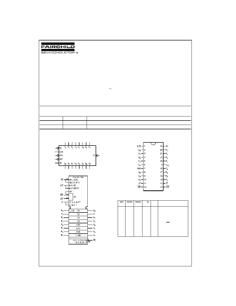
Logic Symbols
IEEE/IEC
Connection Diagram
Function Table
H
=
HIGH Voltage Level
L
=
LOW Voltage Level
X
=
Immaterial
=
Transition LOW-to-HIGH
Order Number
Package Number
Package Description
74F269SC
M24B
24-Lead Small Outline Integrated Circuit (SOIC), JEDEC MS-013, 0.300 Wide
74F269SPC
N24C
24-Lead Plastic Dual-In-Line Package (PDIP), JEDEC MS-001, 0.300 Wide
PE
CEP
CET
U/D
CP
Function
L
X
X
X
Parallel Load All
Flip-Flops
H
H
X
X
Hold
H
X
H
X
Hold (TC Held HIGH)
H
L
L
H
Count Up
H
L
L
L
Count Down
www.fairchildsemi.com
2
74F269
Unit Loading/Fan Out
Logic Diagram
Pin Names
Description
U.L.
Input I
IH
/I
IL
HIGH/LOW
Output I
OH
/I
OL
P
0
≠P
7
Parallel Data Inputs
1.0/1.0
20
µ
A/
-
0.6 mA
PE
Parallel Enable Input (Active LOW)
1.0/1.0
20
µ
A/
-
0.6 mA
U/D
Up-Down Count Control Input
1.0/1.0
20
µ
A/
-
0.6 mA
CEP
Count Enable Parallel Input (Active LOW)
1.0/1.0
20
µ
A/
-
0.6 mA
CET
Count Enable Trickle Input (Active LOW)
1.0/1.0
20
µ
A/
-
0.6 mA
CP
Clock Input
1.0/1.0
20
µ
A/
-
0.6 mA
TC
Terminal Count Output (Active LOW)
5.0/33.3
-
1 mA/20 mA
Q
0
≠Q
7
Flip-Flop Outputs
50/33.3
-
1 mA/20 mA
3
www.fairchildsemi.com
7
4
F269
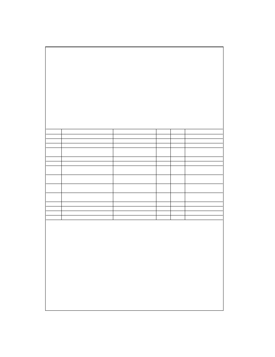
Absolute Maximum Ratings
(Note 1)
Recommended Operating
Conditions
Note 1: Absolute maximum ratings are values beyond which the device
may be damaged or have its useful life impaired. Functional operation
under these conditions is not implied.
Note 2: Either voltage limit or current limit is sufficient to protect inputs.
DC Electrical Characteristics
Storage Temperature
-
65
∞
C to
+
150
∞
C
Ambient Temperature under Bias
-
55
∞
C to
+
125
∞
C
Junction Temperature under Bias
-
55
∞
C to
+
150
∞
C
V
CC
Pin Potential to Ground Pin
-
0.5V to
+
7.0V
Input Voltage (Note 2)
-
0.5V to
+
7.0V
Input Current (Note 2)
-
30 mA to
+
5.0 mA
Voltage Applied to Output
in HIGH State (with V
CC
=
0V)
Standard Output
-
0.5V to V
CC
3-STATE Output
-
0.5V to
+
5.5V
Current Applied to Output
in LOW State (Max)
twice the rated I
OL
(mA)
Free Air Ambient Temperature
0
∞
C to
+
70
∞
C
Supply Voltage
+
4.5V to
+
5.5V
Symbol
Parameter
Min
Typ
Max
Units
V
CC
Conditions
V
IH
Input HIGH Voltage
2.0
V
Recognized as a HIGH Signal
V
IL
Input LOW Voltage
0.8
V
Recognized as a LOW Signal
V
CD
Input Clamp Diode Voltage
-
1.2
V
Min
I
IN
=
-
18 mA
V
OH
Output HIGH
10% V
CC
2.5
V
Min
I
OH
=
-
1 mA
Voltage
5% V
CC
2.7
I
OH
=
-
1 mA
V
OL
Output LOW Voltage
10% V
CC
0.5
V
Min
I
OL
=
20 mA
I
IH
Input HIGH Current
5.0
µ
A
Max
V
IN
=
2.7V
I
BVI
Input HIGH Current
7.0
µ
A
Max
V
IN
=
7.0V
Breakdown Test
I
CEX
Output HIGH
50
µ
A
Max
V
OUT
=
V
CC
Leakage Current
V
ID
Input Leakage Test
4.75
V
0.0
I
ID
=
1.9
µ
A,
All Other Pins Grounded
I
OD
Output Leakage
3.75
µ
A
0.0
V
IOD
=
150 mV
Circuit Current
All Other Pins Grounded
I
IL
Input LOW Current
-
0.6
mA
Max
V
IN
=
0.5V
I
OS
Output Short-Circuit Current
-
60
-
150
mA
Max
V
OUT
=
0V
I
CCH
Power Supply Current
104
125
mA
Max
V
O
=
HIGH
I
CCL
Power Supply Current
113
135
mA
Max
V
O
=
LOW
www.fairchildsemi.com
4
74F269
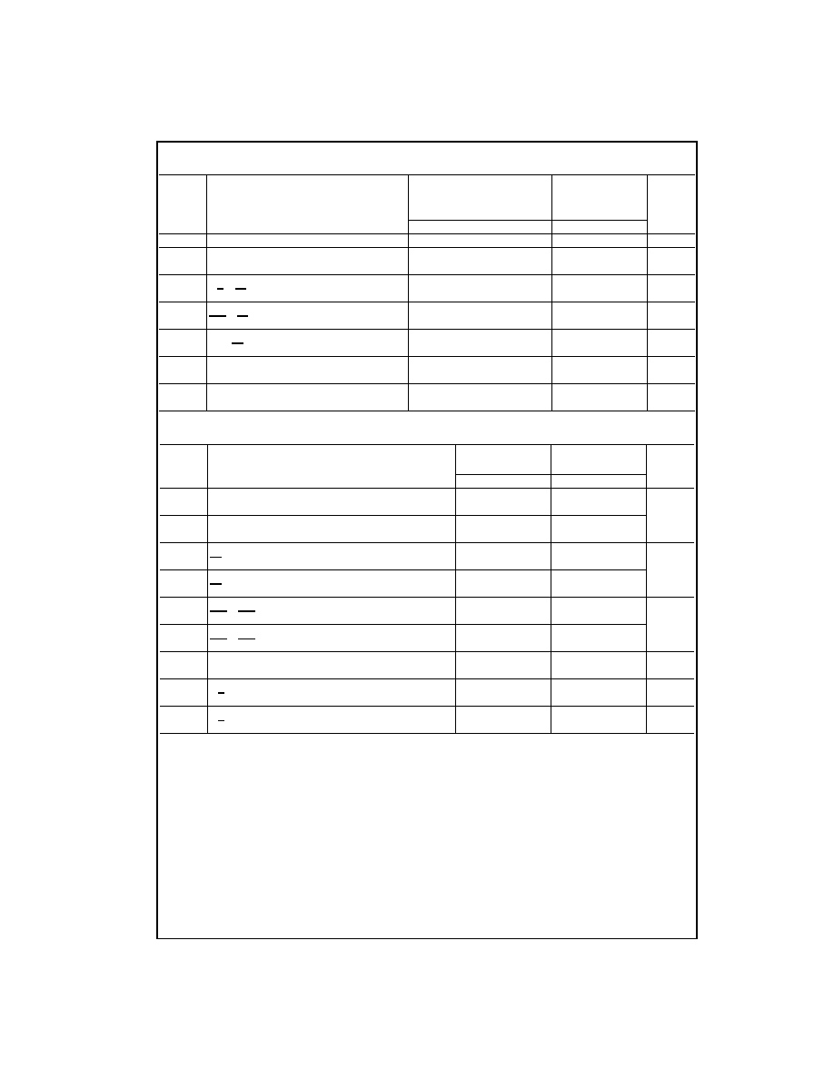
AC Electrical Characteristics
AC Operating Requirements
Symbol
Parameter
T
A
=
+
25
∞
C
T
A
=
0
∞
C to
+
70
∞
C
Units
V
CC
=
+
5.0V
V
CC
=
5.0V
C
L
=
50 pF
C
L
=
50 pF
Min
Typ
Max
Min
Max
f
MAX
Maximum Clock Frequency
100
85
MHz
t
PLH
Propagation Delay
3.5
8.0
3.5
7.0
ns
t
PHL
CP to Q
n
(Count-Up)
4.5
10.5
4.5
11.0
t
PLH
Propagation Delay
3.5
7.5
3.5
10.0
ns
t
PHL
U/D to TC
4.5
7.5
4.5
11.0
t
PLH
Propagation Delay
3.5
7.0
3.5
10.5
ns
t
PHL
CET to TC
3.0
10.5
3.0
11.5
t
PLH
Propagation Delay
4.5
10.0
4.5
10.5
ns
t
PHL
CP to TC
5.0
10.0
4.5
10.5
t
PLH
Propagation Delay
3.5
10.5
3.5
11.0
ns
t
PHL
CP to
Qn
(Count-Down)
4.5
10.5
4.5
11.0
t
PLH
Propagation Delay
3.5
7.0
3.5
10.0
ns
t
PHL
CP to Q
n
(Load)
4.0
7.0
4.0
7.0
Symbol
Parameter
T
A
=
+
25
∞
C
T
A
=
0
∞
C to
+
70
∞
C
Units
V
CC
=
+
5.0V
V
CC
=
5.0V
Min
Max
Min
Max
t
S
(H)
Setup Time, HIGH or LOW
3.5
4.0
ns
t
S
(L)
Data to CP
3.0
3.0
t
H
(H)
Hold Time, HIGH or LOW
1.0
2.0
t
H
(L)
Data to CP
1.0
1.0
t
S
(H)
Setup Time, HIGH or LOW
5.5
6.5
ns
t
S
(L)
PE to CP
5.5
6.5
t
H
(H)
Hold Time, HIGH or LOW
0
0
t
H
(L)
PE to CP
0
0
t
S
(H)
Setup Time, HIGH or LOW
6.0
6.5
ns
t
S
(L)
CET or CEP to CP
8.0
9.0
t
H
(H)
Hold Time, HIGH or LOW
0
0
t
H
(L)
CET or CEP to CP
0
0
t
W
(H)
Clock Pulse Width, HIGH or LOW
3.5
3.5
ns
t
W
(L)
3.5
4.0
t
S
(H)
Setup Time, HIGH or LOW
8.0
9.5
ns
t
S
(L)
U/D to CP
6.0
7.0
t
H
(H)
Hold Time, HIGH or LOW
0.0
0.0
ns
t
H
(L)
U/D to CP
0.0
0.0
5
www.fairchildsemi.com
7
4
F269
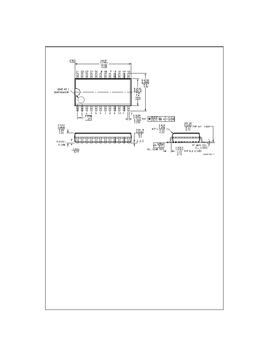
Physical Dimensions
inches (millimeters) unless otherwise noted
28-Lead Small Outline Integrated Circuit (SOIC), JEDEC MS-013, 0.300 Wide
Package Number M24B
www.fairchildsemi.com
6
74F269 8-Bi
t Bidi
rec
t
i
onal Binar
y C
o
u
n
ter
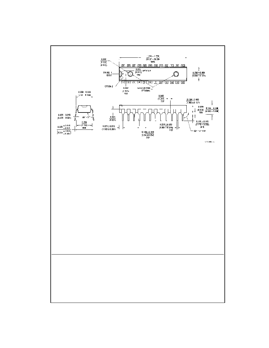
Physical Dimensions
inches (millimeters) unless otherwise noted (Continued)
24-Lead Plastic Dual-In-Line Package (PDIP), JEDEC MS-001, 0.300 Wide
Package Number N24C
Fairchild does not assume any responsibility for use of any circuitry described, no circuit patent licenses are implied and
Fairchild reserves the right at any time without notice to change said circuitry and specifications.
LIFE SUPPORT POLICY
FAIRCHILD'S PRODUCTS ARE NOT AUTHORIZED FOR USE AS CRITICAL COMPONENTS IN LIFE SUPPORT
DEVICES OR SYSTEMS WITHOUT THE EXPRESS WRITTEN APPROVAL OF THE PRESIDENT OF FAIRCHILD
SEMICONDUCTOR CORPORATION. As used herein:
1. Life support devices or systems are devices or systems
which, (a) are intended for surgical implant into the
body, or (b) support or sustain life, and (c) whose failure
to perform when properly used in accordance with
instructions for use provided in the labeling, can be rea-
sonably expected to result in a significant injury to the
user.
2. A critical component in any component of a life support
device or system whose failure to perform can be rea-
sonably expected to cause the failure of the life support
device or system, or to affect its safety or effectiveness.
www.fairchildsemi.com