 | –≠–ª–µ–∫—Ç—Ä–æ–Ω–Ω—ã–π –∫–æ–º–ø–æ–Ω–µ–Ω—Ç: 74F283SJ | –°–∫–∞—á–∞—Ç—å:  PDF PDF  ZIP ZIP |
© 1999 Fairchild Semiconductor Corporation
DS009513
www.fairchildsemi.com
April 1988
Revised August 1999
7
4F283 4-Bi
t Binar
y
Ful
l Adder wit
h
F
ast Carr
y
74F283
4-Bit Binary Full Adder with Fast Carry
General Description
The 74F283 high-speed 4-bit binary full adder with internal
carry lookahead accepts two 4-bit binary words (A
0
≠A
3
,
B
0
≠B
3
) and a Carry input (C
0
). It generates the binary Sum
outputs (S
0
≠S
3
) and the Carry output (C
4
) from the most
significant bit. The 74F283 will operate with either active
HIGH or active LOW operands (positive or negative logic).
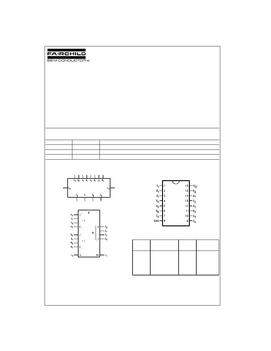
Ordering Code:
Devices also available in Tape and Reel. Specify by appending the suffix letter "X" to the ordering code.
Logic Symbols
IEEE/IEC
Connection Diagram
Unit Loading/Fan Out
Order Number
Package Number
Package Description
74F283SC
M16A
16-Lead Small Outline Integrated Circuit (SOIC), JEDEC MS-012, 0.150 Narrow
74F283SJ
M16D
16-Lead Small Outline Package (SOP), EIAJ TYPE II, 5.3mm Wide
74F283PC
N16E
16-Lead Plastic Dual-In-Line Package (PDIP), JEDEC MS-001, 0.300 Wide
Pin Names
Description
U.L.
Input I
IH
/I
IL
HIGH/LOW Output I
OH
/I
OL
A
0
≠A
3
A Operand Inputs
1.0/2.0
20
µ
A/
-
1.2 mA
B
0
≠B
3
B Operand Inputs
1.0/2.0
20
µ
A/
-
1.2 mA
C
0
Carry Input
1.0/1.0
20
µ
A/
-
0.6 mA
S
0
≠S
3
Sum Outputs
50/33.3
-
1 mA/20 mA
C
4
Carry Output
50/33.3
-
1 mA/20 mA
www.fairchildsemi.com
2
74F283
Functional Description
The 74F283 adds two 4-bit binary words (A plus B) plus the
incoming Carry (C
0
). The binary sum appears on the Sum
(S
0
≠S
3
) and outgoing carry (C
4
) outputs. The binary weight
of the various inputs and outputs is indicated by the sub-
script numbers, representing powers of two.
2
0
(A
0
+
B
0
+
C
0
)
+
2
1
(A
1
+
B
1
)
+
2
2
(A
2
+
B
2
)
+
2
3
(A
3
+
B
3
)
=
S
0
+
2S
1
+
4S
2
+
8S
3
+
16C
4
Where (
+
)
=
plus
Interchanging inputs of equal weight does not affect the
operation. Thus C
0
, A
0
, B
0
can be arbitrarily assigned to
pins 5, 6 and 7 for DIPS, and 7, 8 and 9 for chip carrier
packages. Due to the symmetry of the binary add function,
the 74F283 can be used either with all inputs and outputs
active HIGH (positive logic) or with all inputs and outputs
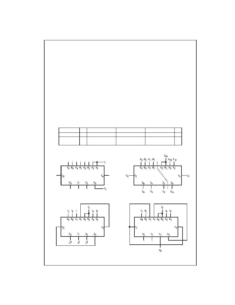
active LOW (negative logic). See Figure 1. Note that if C
0
is
not used it must be tied LOW for active HIGH logic or tied
HIGH for active LOW logic.
Due to pin limitations, the intermediate carries of the
74F283 are not brought out for use as inputs or outputs.
However, other means can be used to effectively insert a
carry into, or bring a carry out from, an intermediate stage.
Figure 2 shows how to make a 3-bit adder. Tying the oper-
and inputs of the fourth adder (A
3
, B
3
) LOW makes S
3
dependent only on, and equal to, the carry from the third
adder. Using somewhat the same principle, Figure 3 shows
a way of dividing the 74F283 into a 2-bit and a 1-bit adder.
The third stage adder (A
2
, B
2
, S
2
) is used merely as a
means of getting a carry (C
10
) signal into the fourth stage
(via A
2
and B
2
) and bringing out the carry from the second
stage on S
2
. Note that as long as A
2
and B
2
are the same,
whether HIGH or LOW, they do not influence S
2
. Similarly,
when A
2
and B
2
are the same the carry into the third stage
does not influence the carry out of the third stage. Figure 4
shows a method of implementing a 5-input encoder, where
the inputs are equally weighted. The outputs S
0
, S
1
and S
2
present a binary number equal to the number of inputs I
1
≠
I
5
that are true. Figure 5 shows one method of implement-
ing a 5-input majority gate. When three or more of the
inputs I
1
≠I
5
are true, the output M
5
is true.
Active HIGH: 0
+
10
+
9
=
3
+
16
Active LOW: 1
+
5
+
6
=
12
+
0
FIGURE 1. Active HIGH versus Active LOW Interpretation
FIGURE 2. 3-Bit Adder
FIGURE 3. 2-Bit and 1-Bit Adders
FIGURE 4. 5-Input Encoder
FIGURE 5. 5-Input Majority Gate
C
0
A
0
A
1
A
2
A
3
B
0
B
1
B
2
B
3
S
0
S
1
S
2
S
3
C
4
Logic Levels
L
L
H
L
H
H
L
L
H
H
H
L
L
H
Active HIGH
0
0
1
0
1
1
0
0
1
1
1
0
0
1
Active LOW
1
1
0
1
0
0
1
1
0
0
0
1
1
0
3
www.fairchildsemi.com
7
4F283
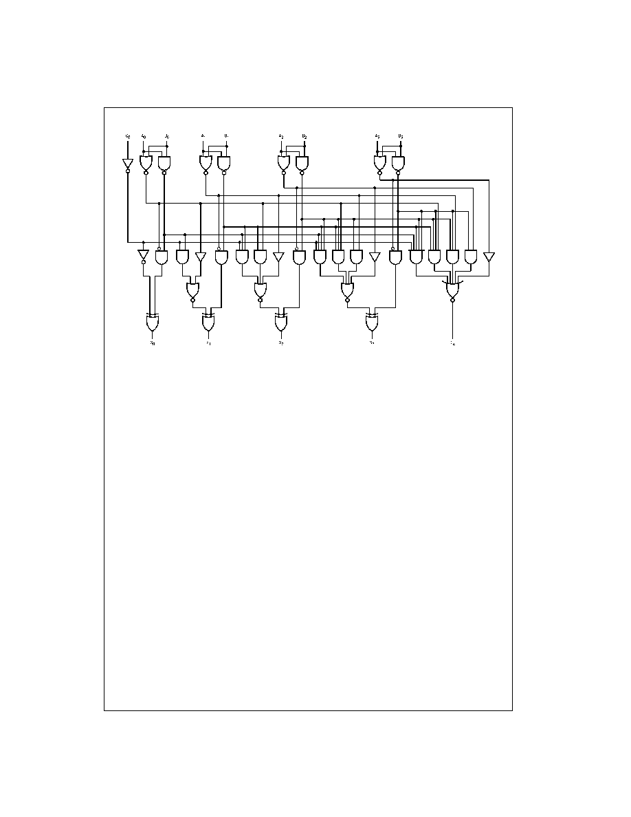
Logic Diagram
Please note that this diagram is provided only for the understanding of logic operations and should not be used to estimate propagation delays.
www.fairchildsemi.com
4
74F283
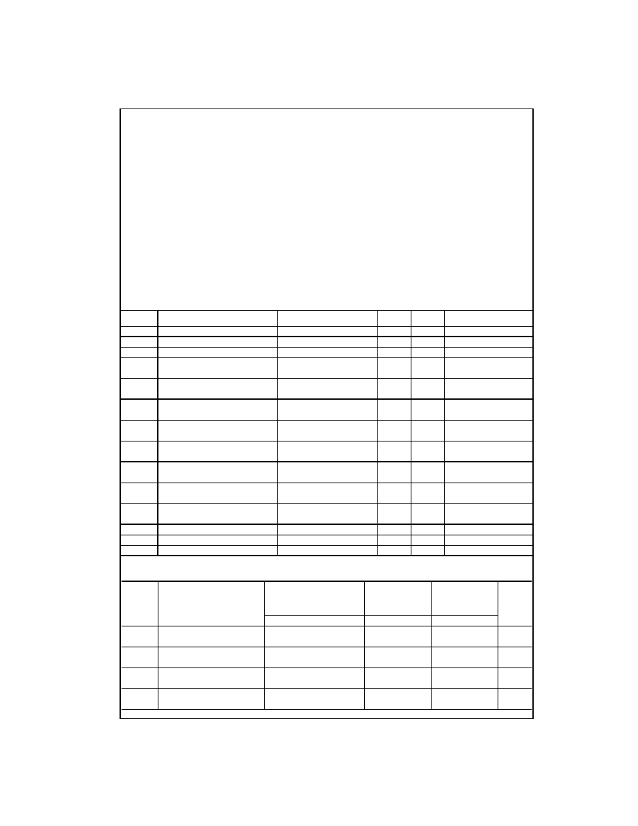
Absolute Maximum Ratings
(Note 1)
Recommended Operating
Conditions
Note 1: Absolute maximum ratings are values beyond which the device
may be damaged or have its useful life impaired. Functional operation
under these conditions is not implied.
Note 2: Either voltage limit or current limit is sufficient to protect inputs.
DC Electrical Characteristics
AC Electrical Characteristics
Storage Temperature
-
65
∞
C to
+
150
∞
C
Ambient Temperature under Bias
-
55
∞
C to
+
125
∞
C
Junction Temperature under Bias
-
55
∞
C to
+
150
∞
C
V
CC
Pin Potential to Ground Pin
-
0.5V to
+
7.0V
Input Voltage (Note 2)
-
0.5V to
+
7.0V
Input Current (Note 2)
-
30 mA to
+
5.0 mA
Voltage Applied to Output
in HIGH State (with V
CC
=
0V)
Standard Output
-
0.5V to V
CC
3-STATE Output
-
0.5V to
+
5.5V
Current Applied to Output
in LOW State (Max)
twice the rated I
OL
(mA)
ESD Last Passing Voltage (Min)
4000V
Free Air Ambient Temperature
0
∞
C to
+
70
∞
C
Supply Voltage
+
4.5V to
+
5.5V
Symbol
Parameter
Min
Typ
Max
Units
V
CC
Conditions
V
IH
Input HIGH Voltage
2.0
V
Recognized as a HIGH Signal
V
IL
Input LOW Voltage
0.8
V
Recognized as a LOW Signal
V
CD
Input Clamp Diode Voltage
-
1.2
V
Min
I
IN
=
-
18 mA
V
OH
Output HIGH
10% V
CC
2.5
V
Min
I
OH
=
-
1 mA
Voltage
5% V
CC
2.7
I
OH
=
-
1 mA
V
OL
Output LOW
10% V
CC
0.5
V
Min
I
OL
=
20 mA
Voltage
I
IH
Input HIGH
5.0
µ
A
Max
V
IN
=
2.7V
Current
I
BVI
Input HIGH Current
7.0
µ
A
Max
V
IN
=
7.0V
Breakdown Test
I
CEX
Output HIGH
50
µ
A
Max
V
OUT
=
V
CC
Leakage Current
V
ID
Input Leakage
4.75
V
0.0
I
ID
=
1.9
µ
A
Test
All Other Pins Grounded
I
OD
Output Leakage
3.75
µ
A
0.0
V
IOD
=
150 mV
Circuit Current
All Other Pins Grounded
I
IL
Input LOW Current
-
0.6
mA
Max
V
IN
=
0.5V (C
O
)
-
1.2
V
IN
=
0.5V (A
n
, B
n
)
I
OS
Output Short-Circuit Current
-
60
-
150
mA
Max
V
OUT
=
0V
I
CCH
Power Supply Current
36
55
mA
Max
V
O
=
HIGH
I
CCL
Power Supply Current
36
55
mA
Max
V
O
=
LOW
Symbol
Parameter
T
A
=
+
25
∞
C
T
A
=
-
55
∞
C to
+
125
∞
C
T
A
=
0
∞
C to
+
70
∞
C
Units
V
CC
=
+
5.0V
V
CC
=
5.0V
V
CC
=
5.0V
C
L
=
50 pF
C
L
=
50 pF
C
L
=
50 pF
Min
Typ
Max
Min
Max
Min
Max
t
PLH
Propagation Delay
3.5
7.0
9.5
3.5
14.0
3.5
11.0
ns
t
PHL
C
0
to S
n
3.0
7.0
9.5
3.0
14.0
3.0
11.0
t
PLH
Propagation Delay
3.0
7.0
9.5
3.0
17.0
3.0
13.0
ns
t
PHL
A
n
or B
n
to S
n
3.0
7.0
9.5
3.0
14.0
3.0
11.5
t
PLH
Propagation Delay
3.0
5.7
7.5
3.0
10.5
3.0
8.5
ns
t
PHL
C
0
to C
4
3.0
5.4
7.0
2.5
10.0
3.0
8.0
t
PLH
Propagation Delay
3.0
5.7
7.5
3.0
10.5
3.0
8.5
ns
t
PHL
A
n
or B
n
to C
4
2.5
5.3
7.0
2.5
10.0
2.5
8.0
5
www.fairchildsemi.com
7
4F283
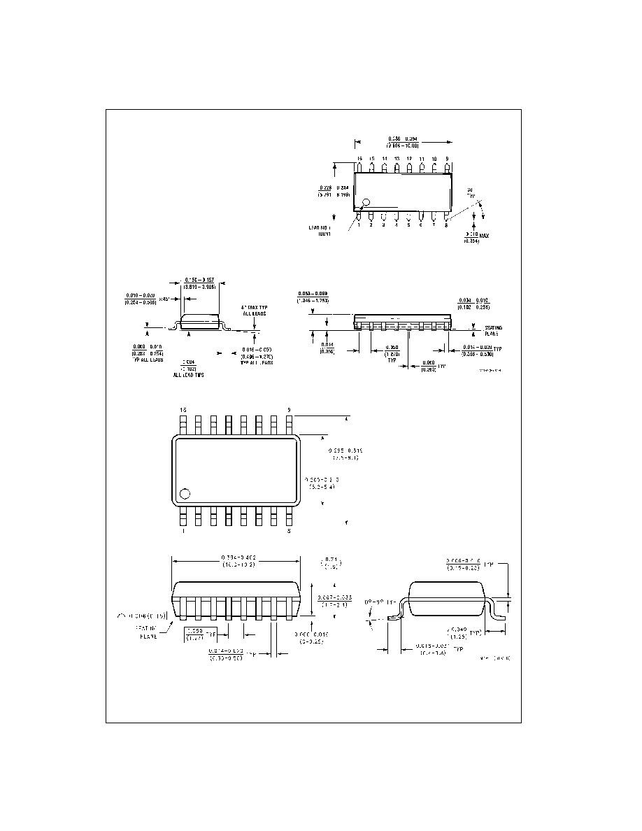
Physical Dimensions
inches (millimeters) unless otherwise noted
16-Lead Small Outline Integrated Circuit (SOIC), JEDEC MS-012, 0.150 Narrow
Package Number M16A
16-Lead Small Outline Package (SOP), EIAJ TYPE II, 5.3mm Wide
Package Number M16D

www.fairchildsemi.com
6
74
F283
4
-
Bit
B
i
nar
y
Ful
l Adder wit
h
Fa
st Carry
Physical Dimensions
inches (millimeters) unless otherwise noted (Continued)
16-Lead Plastic Dual-In-Line Package (PDIP), JEDEC MS-001, 0.300 Wide
Package Number N16E
Fairchild does not assume any responsibility for use of any circuitry described, no circuit patent licenses are implied and
Fairchild reserves the right at any time without notice to change said circuitry and specifications.
LIFE SUPPORT POLICY
FAIRCHILD'S PRODUCTS ARE NOT AUTHORIZED FOR USE AS CRITICAL COMPONENTS IN LIFE SUPPORT
DEVICES OR SYSTEMS WITHOUT THE EXPRESS WRITTEN APPROVAL OF THE PRESIDENT OF FAIRCHILD
SEMICONDUCTOR CORPORATION. As used herein:
1. Life support devices or systems are devices or systems
which, (a) are intended for surgical implant into the
body, or (b) support or sustain life, and (c) whose failure
to perform when properly used in accordance with
instructions for use provided in the labeling, can be rea-
sonably expected to result in a significant injury to the
user.
2. A critical component in any component of a life support
device or system whose failure to perform can be rea-
sonably expected to cause the failure of the life support
device or system, or to affect its safety or effectiveness.
www.fairchildsemi.com