 | –≠–ª–µ–∫—Ç—Ä–æ–Ω–Ω—ã–π –∫–æ–º–ø–æ–Ω–µ–Ω—Ç: 74F322 | –°–∫–∞—á–∞—Ç—å:  PDF PDF  ZIP ZIP |
April 1988
Revised April 1999
7
4F322 O
c
t
a
l
Seri
al
/Par
all
e
l Regi
ster
wi
th Sign Exten
d
© 1999 Fairchild Semiconductor Corporation
DS009516.prf
www.fairchildsemi.com
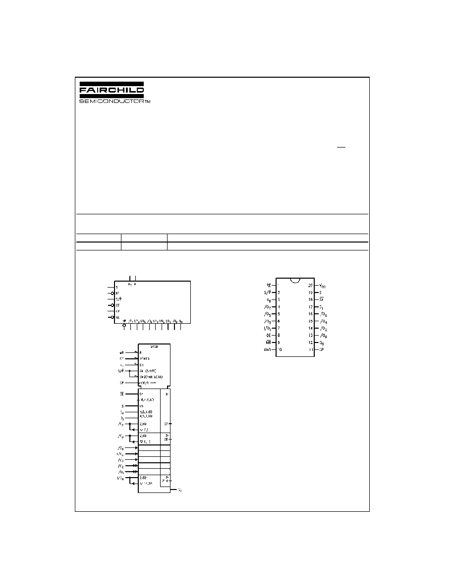
74F322
Octal Serial/Parallel Register with Sign Extend
General Description
The 74F322 is an 8-bit shift register with provision for either
serial or parallel loading and with 3-STATE parallel outputs
plus a bi-state serial output. Parallel data inputs and paral-
lel outputs are multiplexed to minimize pin count. State
changes are initiated by the rising edge of the clock. Four
synchronous modes of operation are possible: hold (store),
shift right with serial entry, shift right with sign extend and
parallel load. An asynchronous Master Reset (MR) input
overrides clocked operation and clears the register.
Features
s
Multiplexed parallel I/O ports
s
Separate serial input and output
s
Sign extend function
s
3-STATE outputs for bus applications
Ordering Code:
Devices also available in Tape and Reel. Specify by appending the suffix letter "X" to the ordering code.
Logic Symbols
IEEE/IEC
Connection Diagram
Order Number
Package Number
Package Description
74F322PC
N20A
20-Lead Plastic Dual-In-Line Package (PDIP), JEDEC MS-001, 0.300 Wide
www.fairchildsemi.com
2
74F322
Unit Loading/Fan Out
Functional Description
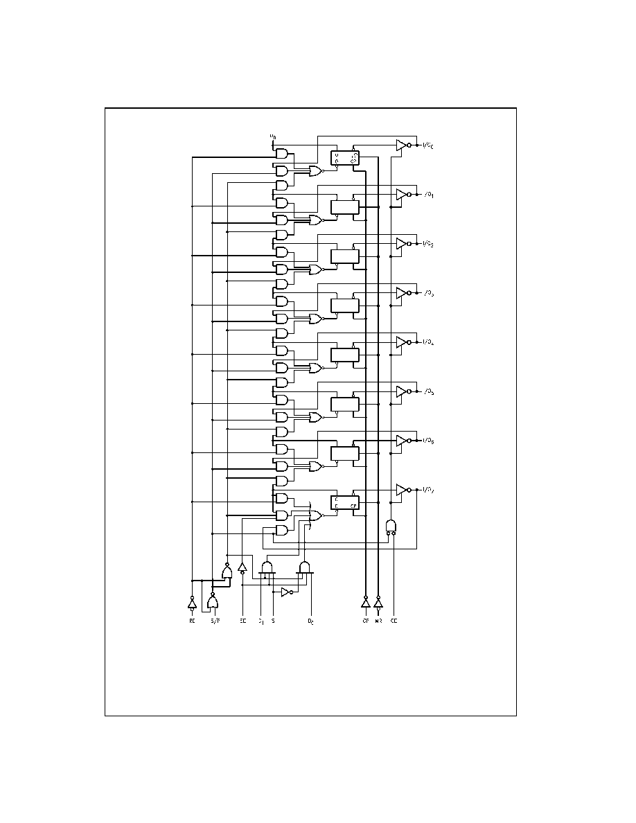
The 74F322 contains eight D-type edge triggered flip-flops
and the interstage gating required to perform right shift and
the intrastage gating necessary for hold and synchronous
parallel load operations. A LOW signal on RE enables shift-
ing or parallel loading, while a HIGH signal enables the
hold mode. A HIGH signal on S/P enables shift right, while
a LOW signal disables the 3-STATE output buffers and
enables parallel loading. In the shift right mode a HIGH sig-
nal on SE enables serial entry from either D
0
or D
1
, as
determined by the S input. A LOW signal on SE enables
shift right but Q
7
reloads its contents, thus performing the
sign extend function required for the 74F384 Twos Com-
plement Multiplier. A HIGH signal on OE disables the 3-
STATE output buffers, regardless of the other control
inputs. In this condition the shifting and loading operations
can still be performed.
Mode Select Table
H
=
HIGH Voltage Level
L
=
LOW Voltage Level
Z
=
High Impedance Output State
=
LOW-to-HIGH Transition
NC
=
No Change
Note: I
7
≠I
0
=
The level of the steady-state input at the respective I/O terminal is loaded into the flip-flop while the flip-flop outputs (except Q
0
) are isolated
from the I/O terminal.
Note: D
0
, D
1
=
The level of the steady-state inputs to the serial multiplexer input.
Note: O
7
≠O
0
=
The level of the respective Q
n
flip-flop prior to the last Clock LOW-to-HIGH transition.
Note 1: When the OE input is HIGH all I/O
n
terminals are at the high impedance state; sequential operation or clearing of the register is not affected.
Pin Names
Description
U.L.
Input I
IH
/I
IL
HIGH/LOW
Output I
OH
/I
OL
RE
Register Enable Input (Active LOW)
1.0/1.0
20
µ
A/
-
0.6 mA
S/P
Serial (HIGH) or Parallel (LOW) Mode Control Input
1.0/1.0
20
µ
A/
-
0.6 mA
SE
Sign Extend Input (Active LOW)
1.0/3.0
20
µ
A/
-
1.8 mA
S
Serial Data Select Input
1.0/2.0
20
µ
A/
-
1.2 mA
D
0
, D
1
Serial Data Inputs
1.0/1.0
20
µ
A/
-
0.6 mA
CP
Clock Pulse Input (Active Rising Edge)
1.0/1.0
20
µ
A/
-
0.6 mA
MR
Asynchronous Master Reset Input (Active LOW)
1.0/1.0
20
µ
A/
-
0.6 mA
OE
3-STATE Output Enable Input (Active LOW)
1.0/1.0
20
µ
A/
-
0.6 mA
Q
0
Bi-State Serial Output
50/33.3
-
1 mA/
-
20 mA
I/O
0
≠I/O
7
Multiplexed Parallel Data Inputs or
3.5/1.083
70
µ
A/
-
0.65 mA
3-STATE Parallel Data Outputs
150/40 (33.3)
-
3 mA/24 mA (20 mA)
Mode
Inputs
Outputs
Q
0
MR
RE
S/P
SE
S
OE
(Note 1)
CP
I/O
7
I/O
6
I/O
5
I/O
4
I/O
3
I/O
2
I/O
1
I/O
0
Clear
L
X
X
X
X
L
X
L
L
L
L
L
L
L
L
L
L
X
X
X
X
H
X
Z
Z
Z
Z
Z
Z
Z
Z
L
Parallel
H
L
L
X
X
X
I
7
I
6
I
5
I
4
I
3
I
2
I
1
I
0
I
0
Load
Shift
H
L
H
H
L
L
D
0
O
7
O
6
O
5
O
4
O
3
O
2
O
1
O
1
Right
H
L
H
H
H
L
D
1
O
7
O
6
O
5
O
4
O
3
O
2
O
1
O
1
Sign
H
L
H
L
X
L
O
7
O
7
O
6
O
5
O
4
O
3
O
2
O
1
O
1
Extend
Hold
H
H
X
X
X
L
NC
NC
NC
NC
NC
NC
NC
NC
NC
3
www.fairchildsemi.com
7
4F322
Logic Diagram
Please note that this diagram is provided only for the understanding of logic operations and should not be used to estimate propagation delays.

www.fairchildsemi.com
4
74F322
Absolute Maximum Ratings
(Note 2)
Recommended Operating
Conditions
Note 2: Absolute maximum ratings are values beyond which the device
may be damaged or have its useful life impaired. Functional operation
under these conditions is not implied.
Note 3: Either voltage limit or current limit is sufficient to protect inputs.
DC Electrical Characteristics
Storage Temperature
-
65
∞
C to
+
150
∞
C
Ambient Temperature under Bias
-
55
∞
C to
+
125
∞
C
Junction Temperature under Bias
-
55
∞
C to
+
150
∞
C
V
CC
Pin Potential to Ground Pin
-
0.5V to
+
7.0V
Input Voltage (Note 3)
-
0.5V to
+
7.0V
Input Current (Note 3)
-
30 mA to
+
5.0 mA
Voltage Applied to Output
in HIGH State (with V
CC
=
0V)
Standard Output
-
0.5V to V
CC
3-STATE Output
-
0.5V to
+
5.5V
Current Applied to Output
in LOW State (Max)
twice the rated I
OL
(mA)
Free Air Ambient Temperature
0
∞
C to
+
70
∞
C
Supply Voltage
+
4.5V to
+
5.5V
Symbol
Parameter
Min
Typ
Max
Units
V
CC
Conditions
V
IH
Input HIGH Voltage
2.0
V
Recognized as a HIGH Signal
V
IL
Input LOW Voltage
0.8
V
Recognized as a LOW Signal
V
CD
Input Clamp Diode Voltage
-
1.2
V
Min
I
IN
=
-
18 mA
V
OH
Output HIGH Voltage
10% V
CC
2.5
V
Min
I
OH
=
-
1 mA (Q
0
, I/O
n
)
10% V
CC
2.4
I
OH
=
-
3 mA (I/O
n
)
5% V
CC
2.7
I
OH
=
-
1 mA (Q
0
, I/O
n
)
5% V
CC
2.7
I
OH
=
-
3 mA (I/O
n
)
V
OL
Output LOW Voltage
10% V
CC
0.5
V
Min
I
OL
=
20 mA (Q
0
)
10% V
CC
0.5
I
OL
=
24 mA (I/O
n
)
I
IH
Input HIGH Current
5.0
µ
A
Max
V
IN
=
2.7V
I
BVI
Input HIGH Current Breakdown Test
7.0
µ
A
Max
V
IN
=
7.0V (Non-I/O Inputs)
I
BVIT
Input HIGH Current Breakdown Test (I/O)
0.5
mA
Max
V
IN
=
5.5V (I/O
n
)
I
CEX
Output HIGH Leakage Current
50
µ
A
Max
V
OUT
=
V
CC
V
ID
Input Leakage
4.75
V
0.0
I
ID
=
1.9
µ
A
Test
All Other Pins Grounded
I
OD
Output Leakage
3.75
µ
A
0.0
V
IOD
=
150 mV
Circuit Current
All Other Pins Grounded
I
IL
Input LOW Current
-
0.6
mA
Max
V
IN
=
0.5V (RE, S/P, D
n
, CP, MR, OE)
-
1.2
mA
Max
V
IN
=
0.5V (S)
-
1.8
mA
Max
V
IN
=
0.5V (SE)
I
IH
+
Output Leakage Current
70
µ
A
Max
V
I/O
=
2.7V (I/O
n
)
I
OZH
I
IL
+
Output Leakage Current
-
650
µ
A
Max
V
I/O
=
0.5V (I/O
n
)
I
OZL
I
OS
Output Short-Circuit Current
-
60
-
150
mA
Max
V
OUT
=
0V
I
ZZ
Bus Drainage Test
500
µ
A
0.0V
V
OUT
=
5.25V
I
CC
Power Supply Current
60
90
mA
Max
5
www.fairchildsemi.com
7
4F322
AC Electrical Characteristics
AC Operating Requirements
Symbol
Parameter
T
A
=
+
25
∞
C
T
A
=
-
55
∞
C to
+
125
∞
C
T
A
=
0
∞
C to
+
75
∞
C
Units
V
CC
=
+
5.0V
C
L
=
50 pF
C
L
=
50 pF
C
L
=
50 pF
Min
Typ
Max
Min
Max
Min
Max
f
MAX
Maximum Clock Frequency
70
90
50
70
MHz
t
PLH
Propagation Delay
3.5
7.0
7.5
3.5
9.5
3.5
8.5
ns
t
PHL
CP to I/O
n
5.0
8.5
11.0
3.5
10.0
5.0
12.0
t
PLH
Propagation Delay
3.5
7.0
9.0
3.5
11.0
3.5
10.0
t
PHL
CP to Q
0
3.5
7.0
8.0
3.5
10.0
3.5
9.0
t
PHL
Propagation Delay
6.0
10.0
13.0
6.0
15.0
6.0
14.0
ns
MR to I/O
n
t
PHL
Propagation Delay
5.5
7.5
12.0
5.5
14.0
5.5
13.0
ns
MR to Q
0
t
PZH
Output Enable Time
3.0
6.5
9.0
3.0
12.5
3.0
10.0
ns
t
PZL
OE to I/O
n
4.0
8.5
11.0
4.0
14.5
4.0
12.0
t
PHZ
Output Disable Time
2.0
4.5
6.0
2.0
8.0
2.0
7.0
t
PLZ
OE to I/O
n
2.0
5.0
7.0
2.0
10.0
2.0
8.0
t
PZH
Output Enable Time
4.5
8.0
10.5
4.5
13.5
4.5
11.5
ns
t
PZL
S/P to I/O
n
5.5
10.0
14.0
5.5
17.0
5.5
15.0
t
PHZ
Output Disable Time
5.0
9.0
11.5
5.0
16.5
5.0
12.5
t
PLZ
S/P to I/O
n
6.0
12.0
15.5
6.0
19.5
6.0
16.5
Symbol
Parameter
T
A
=
+
25
∞
C
T
A
=
-
55
∞
C to
+
125
∞
C
T
A
=
0C to
+
75
∞
C
Units
V
CC
=
+
5.0V
Min
Max
Min
Max
Min
Max
t
S
(H)
Setup Time, HIGH or LOW
6.0
14.0
7.0
ns
t
S
(L)
RE to CP
14.0
18.0
16.0
t
H
(H)
Hold Time, HIGH or LOW
0
0
0
ns
t
H
(L)
RE to CP
0
0
0
t
S
(H)
Setup Time, HIGH or LOW
6.5
8.5
7.5
ns
t
S
(L)
D
0
, D
1
or I/O
n
to CP
6.5
8.5
7.5
t
H
(H)
Hold Time, HIGH or LOW
2.0
3.0
3.0
ns
t
H
(L)
D
0
, D
1
or I/O
n
to CP
2.0
3.0
3.0
t
S
H)
Setup Time, HIGH or LOW
7.0
9.0
8.0
ns
t
S
(L)
SE to CP
2.5
11.0
3.5
t
H
(H)
Hold Time, HIGH or LOW
2.0
2.0
2.0
ns
t
H
(L)
SE to CP
0.0
1.0
0.0
t
S
(H)
Setup Time, HIGH or LOW
11.0
13.0
12.0
ns
t
S
(L)
S/P to CP
13.5
21.0
15.5
t
S
(H)
Setup Time, HIGH or LOW
6.5
8.5
7.5
ns
t
S
(L)
S to CP
9.0
11.0
10.0
t
H
(H)
Hold Time, HIGH or LOW
0
1.0
0
ns
t
H
(L)
S or S/P to CP
0
0
0
t
W
(H)
CP Pulse Width, HIGH or LOW
7.0
8.0
7.0
ns
t
W
(L)
t
W
(L)
MR Pulse Width, LOW
5.5
7.5
6.5
t
REC
Recovery Time
8.0
12.0
8.0
ns
MR to CP