 | –≠–ª–µ–∫—Ç—Ä–æ–Ω–Ω—ã–π –∫–æ–º–ø–æ–Ω–µ–Ω—Ç: 74F323SC | –°–∫–∞—á–∞—Ç—å:  PDF PDF  ZIP ZIP |
© 1999 Fairchild Semiconductor Corporation
DS009517
www.fairchildsemi.com
April 1988
Revised August 1999
7
4F323
O
c
t
a
l
Uni
versal
Shi
f
t
/
S
t
o
ra
ge Regi
ste
r
74F323
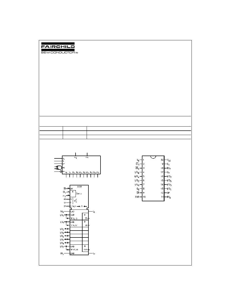
Octal Universal Shift/Storage Register
with Synchronous Reset and Common I/O Pins
General Description
The 74F323 is an 8-bit universal shift/storage register with
3-STATE outputs. Its function is similar to the 74F299 with
the exception of Synchronous Reset. Parallel load inputs
and flip-flop outputs are multiplexed to minimize pin count.
Separate serial inputs and outputs are provided for Q
0
and
Q
7
to allow easy cascading. Four operation modes are
possible: hold (store), shift left, shift right and parallel load.
Features
s
Common parallel I/O for reduced pin count
s
Additional serial inputs and outputs for expansion
s
Four operating modes: shift left, shift right, load and
store
s
3-STATE outputs for bus-oriented applications
Ordering Code:
Devices also available in Tape and Reel. Specify by appending the suffix letter "X" to the ordering code.
Logic Symbols
IEEE/IEC
Connection Diagram
Order Number
Package Number
Package Description
74F323SC
M20B
20-Lead Small Outline Integrated Circuit (SOIC), JEDEC MS-013, 0.300 Wide
74F323PC
N20A
20-Lead Plastic Dual-In-Line Package (PDIP), JEDEC MS-001, 0.300 Wide
www.fairchildsemi.com
2
74F323
Unit Loading/Fan Out
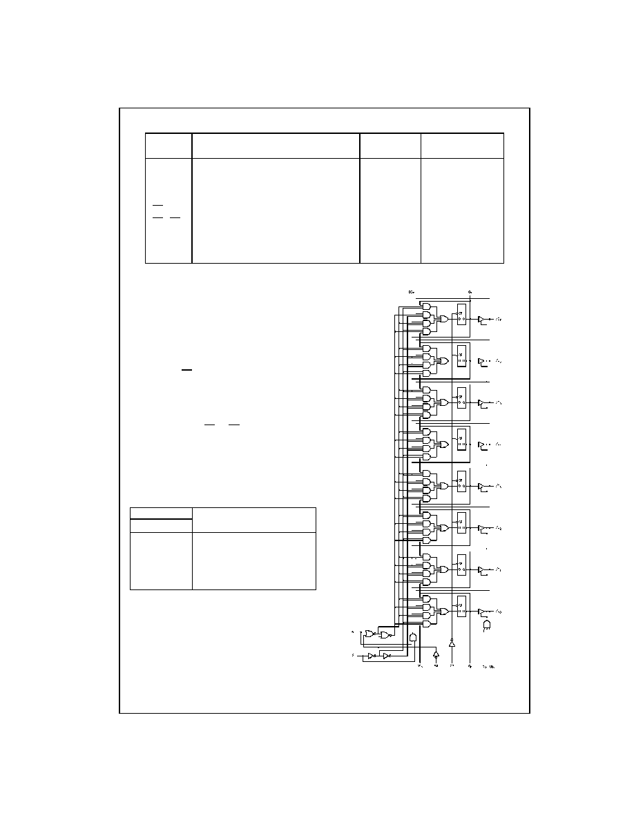
Functional Description
The 74F323 contains eight edge-triggered D-type flip-flops
and the interstage logic necessary to perform synchronous
reset, shift left, shift right, parallel load and hold operations.
The type of operation is determined by S
0
and S
1
as shown
in the Mode Select Table. All flip-flop outputs are brought
out through 3-STATE buffers to separate I/O pins that also
serve as data inputs in the parallel load mode. Q
0
and Q
7
are also brought out on other pins for expansion in serial
shifting of longer words.
A LOW signal on SR overrides the Select inputs and allows
the flip-flops to be reset by the next rising edge of CP. All
other state changes are also initiated by the LOW-to-HIGH
CP transition. Inputs can change when the clock is in either
state provided only that the recommended setup and hold
times, relative to the rising edge of CP, are observed.
A HIGH signal on either OE
1
or OE
2
disables the 3-STATE
buffers and puts the I/O pins in the high impedance state.
In this condition the shift, load, hold and reset operations
can still occur. The 3-STATE buffers are also disabled by
HIGH signals on both S
0
and S
1
in preparation for a paral-
lel load operation.
Mode Select Table
H
=
HIGH Voltage Level
L
=
LOW Voltage Level
X
=
Immaterial
=
LOW-to-HIGH transition
Logic Diagram
Please note that this diagram is provided only for the understanding of logic
operations and should not be used to estimate propagation delays.
Pin Names
Description
U.L.
Input I
IH
/I
IL
HIGH/LOW
Output I
OH
/I
OL
CP
Clock Pulse Input (Active Rising Edge)
1.0/1.0
20
µ
A/
-
0.6 mA
DS
0
Serial Data Input for Right Shift
1.0/1.0
20
µ
A/
-
0.6 mA
DS
7
Serial Data Input for Left Shift
1.0/1.0
20
µ
A/
-
0.6 mA
S
0,
S
1
Mode Select Inputs
1.0/2.0
20
µ
A/
-
1.2 mA
SR
Synchronous Reset Input (Active LOW)
1.0/1.0
20
µ
A/
-
0.6 mA
OE
1,
OE
2
3-STATE Output Enable Inputs (Active LOW)
1.0/1.0
20
µ
A/
-
0.6 mA
I/O
0
≠I/O
7
Multiplexed Parallel Data Inputs
3.5/1.083
70
µ
A/
-
0.65 mA
3-STATE Parallel Data Outputs
150/40 (33.3)
-
3 mA/24 mA (20 mA)
Q
0,
Q
7
Serial Outputs
50/33.3
-
1 mA/20 mA
Inputs
Response
SR S
1
S
0
CP
L
X
X
Synchronous Reset; Q
0
≠Q
7
=
LOW
H
H
H
Parallel Load; I/O
n
Q
n
H
L
H
Shift Right; DS
0
Q
0,
Q
0
Q
1,
etc.
H
H
L
Shift Left; DS
7
Q
7,
Q
7
Q
6,
etc.
H
L
L
X
Hold
3
www.fairchildsemi.com
7
4F323
Absolute Maximum Ratings
(Note 1)
Recommended Operating
Conditions
Note 1: Absolute maximum ratings are values beyond which the device
may be damaged or have its useful life impaired. Functional operation
under these conditions is not implied.
Note 2: Either voltage limit or current limit is sufficient to protect inputs.
DC Electrical Characteristics
Storage Temperature
-
65
∞
C to
+
150
∞
C
Ambient Temperature under Bias
-
55
∞
C to
+
125
∞
C
Junction Temperature under Bias
-
55
∞
C to
+
150
∞
C
V
CC
Pin Potential to Ground Pin
-
0.5V to
+
7.0V
Input Voltage (Note 2)
-
0.5V to
+
7.0V
Input Current (Note 2)
-
30 mA to
+
5.0 mA
Voltage Applied to Output
in HIGH State (with V
CC
=
0V)
Standard Output
-
0.5V to V
CC
3-STATE Output
-
0.5V to
+
5.5V
Current Applied to Output
in LOW State (Max)
twice the rated I
OL
(mA)
ESD Last Passing Voltage (Min)
4000V
Free Air Ambient Temperature
0
∞
C to
+
70
∞
C
Supply Voltage
+
4.5V to
+
5.5V
Symbol
Parameter
Min
Typ
Max
Units
V
CC
Conditions
V
IH
Input HIGH Voltage
2.0
V
Recognized as a HIGH Signal
V
IL
Input LOW Voltage
0.8
V
Recognized as a LOW Signal
V
CD
Input Clamp Diode Voltage
-
1.2
V
Min
I
IN
=
-
18 mA
V
OH
Output HIGH
10% V
CC
2.5
V
Min
I
OH
=
-
1 mA
(Q
0
, Q
7
)
Voltage
10% V
CC
2.4
I
OH
=
-
3 mA
(I/O
n
)
5% V
CC
2.7
I
OH
=
-
1 mA
(Q
0
, Q
7
)
5% V
CC
2.7
I
OH
=
-
3 mA
(I/O
n
)
V
OL
Output LOW
10% V
CC
0.5
V
Min
I
OL
=
20 mA
(Q
0
, Q
7
)
Voltage
10% V
CC
0.5
I
OL
=
24 mA
(I/O
n
)
I
IH
Input HIGH Current
5.0
µ
A
Max
V
IN
=
2.7V
I
BVI
Input HIGH Current
7.0
µ
A
Max
V
IN
=
7.0V (Non I/O Inputs)
Breakdown Test
I
BVIT
Input HIGH Current
0.5
mA
Max
V
IN
=
5.5V (I/O Inputs)
Breakdown (I/O)
I
CEX
Output HIGH
50
µ
A
Max
V
OUT
=
V
CC
Leakage Current
V
ID
Input Leakage
4.75
V
0.0
I
ID
=
1.9
µ
A
Test
All Other Pins Grounded
I
OD
Output Leakage
3.75
µ
A
0.0
V
IOD
=
150 mV
Circuit Current
All Other Pins Grounded
I
IL
Input LOW Current
-
0.6
mA
Max
V
IN
=
0.5V
(CP, DS
0
, DS
7
, SR, OE
1
, OE
2
)
-
1.2
mA
Max
V
IN
=
0.5V
(S
0
, S
1
)
I
OS
Output Short-Circuit Current
-
60
-
150
mA
Max
V
OUT
=
0V
I
ZZ
Bus Drainage Test
500
µ
A
0.0V
V
OUT
=
5.25V
I
CCH
Power Supply Current
68
95
mA
Max
V
O
=
HIGH
I
CCL
Power Supply Current
68
95
mA
Max
V
O
=
LOW
I
CCZ
Power Supply Current
68
95
mA
Max
V
O
=
HIGH Z
www.fairchildsemi.com
4
74F323
AC Electrical Characteristics
AC Operating Requirements
Symbol
Parameter
T
A
=
+
25
∞
C
T
A
=
0
∞
C to
+
70
∞
C
Units
V
CC
=
+
5.0V
V
CC
=
+
5.0V
C
L
=
50 pF
C
L
=
50 pF
Min
Typ
Max
Min
Max
f
MAX
Maximum Input Frequency
70
100
70
MHz
t
PLH
Propagation Delay
4.0
7.0
8.0
4.0
8.5
ns
t
PHL
CP to Q
0
or Q
7
4.5
6.5
8.0
4.5
8.5
t
PLH
Propagation Delay
3.5
7.0
9.0
3.5
10.0
t
PHL
CP to I/O
n
4.0
8.5
9.0
4.0
10.0
t
PZH
Output Enable Time
3.5
6.0
8.0
3.5
9.0
ns
t
PZL
4.0
7.0
10.0
4.0
11.0
t
PHZ
Output Disable Time
2.0
4.5
6.0
2.0
7.0
t
PLZ
1.0
4.0
5.5
1.0
6.5
t
PZH
Output Enable Time
3.5
9.0
3.5
10.0
ns
t
PZL
S
n
to I/O
n
4.0
10.0
4.0
11.0
t
PHZ
Output Disable Time
2.5
6.0
2.5
7.0
ns
t
PLZ
S
n
to I/O
n
1.0
5.5
1.5
6.5
Symbol
Parameter
T
A
=
+
25
∞
C
T
A
=
0
∞
C to
+
70
∞
C
Units
V
CC
=
+
5.0V
V
CC
=
+
5.0V
Min
Max
Min
Max
t
S
(H)
Setup Time, HIGH or LOW
8.5
8.5
ns
t
S
(L)
S
0
or S
1
to CP
8.5
8.5
t
H
(H)
Hold Time, HIGH or LOW
0
0
t
H
(L)
S
0
or S
1
to CP
0
0
t
S
(H)
Setup Time, HIGH or LOW
5.0
5.0
ns
t
S
(L)
I/O
n
, DS
0
, DS
7
to CP
5.0
5.0
t
H
(H)
Hold Time, HIGH or LOW
2.0
2.0
t
H
(L)
I/O
n
, DS
0
, DS
7
to CP
2.0
2.0
t
S
(H)
Setup Time, HIGH or LOW
10.0
10.0
ns
t
S
(L)
SR to CP
10.0
10.0
t
H
(H)
Hold Time, HIGH or LOW
0
0
t
H
(L)
SR to CP
0
0
t
W
(H)
CP Pulse Width
5.0
5.0
ns
t
W
(L)
HIGH or LOW
5.0
5.0
5
www.fairchildsemi.com
7
4F323
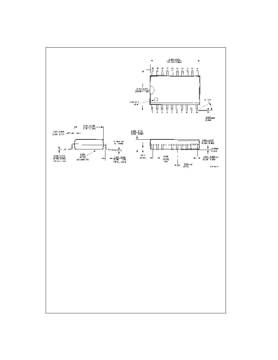
Physical Dimensions
inches (millimeters) unless otherwise noted
20-Lead Small Outline Integrated Circuit (SOIC), JEDEC MS-013, 0.300 Wide
Package Number M20B