 | –≠–ª–µ–∫—Ç—Ä–æ–Ω–Ω—ã–π –∫–æ–º–ø–æ–Ω–µ–Ω—Ç: 74F365 | –°–∫–∞—á–∞—Ç—å:  PDF PDF  ZIP ZIP |
© 1999 Fairchild Semiconductor Corporation
DS009522
www.fairchildsemi.com
April 1988
Revised August 1999
7
4F365
H
e
x Buf
f
er
/Dri
ver
wit
h
3-ST
A
T
E Outp
uts
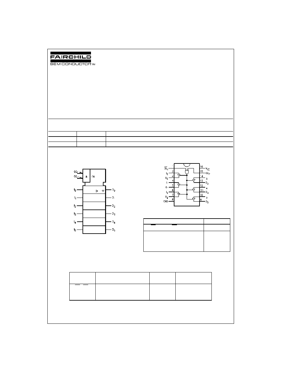
74F365
Hex Buffer/Driver with 3-STATE Outputs
General Description
The 74F365 is a hex buffer and line driver designed to be
employed as a memory and address driver, clock driver
and bus-oriented transmitter/receiver.
Features
s
3-STATE buffer outputs
s
Outputs sink 64 mA
s
Bus-oriented
Ordering Code:
Devices also available in Tape and Reel. Specify by appending the suffix letter "X" to the ordering code.
Logic Symbol
IEEE/IEC
Connection Diagram
Function Table
L
=
LOW Voltage Level
X
=
Immaterial
H
=
HIGH Voltage Level
Z
=
High Impedance
Unit Loading/Fan Out
Order Number
Package Number
Package Description
74F365SC
M16A
16-Lead Small Outline Integrated Circuit (SOIC), JEDEC MS-012, 0.150 Narrow
74F365PC
N16E
16-Lead Plastic Dual-In-Line Package (PDIP), JEDEC MS-001, 0.300 Wide
Inputs
Output
OE
1
OE
2
I
O
L
L
L
L
L
L
H
H
X
H
X
Z
H
X
X
Z
Pin Names
Description
U.L.
Input I
IH
/I
IL
HIGH/LOW
Output I
OH
/I
OL
OE
1
, OE
2
Output Enable Input (Active LOW)
1.0/0.033
20
µ
A/20
µ
A
I
n
Inputs
1.0/0.033
20
µ
A/20
µ
A
O
n
Outputs
600/106.6 (80)
-
12 mA/64 mA (48 mA)
www.fairchildsemi.com
2
74F365
Absolute Maximum Ratings
(Note 1)
Recommended Operating
Conditions
Note 1: Absolute maximum ratings are values beyond which the device
may be damaged or have its useful life impaired. Functional operation
under these conditions is not implied.
Note 2: Either voltage limit or current limit is sufficient to protect inputs.
DC Electrical Characteristics
AC Electrical Characteristics
Storage Temperature
-
65
∞
C to
+
150
∞
C
Ambient Temperature under Bias
-
55
∞
C to
+
125
∞
C
Junction Temperature under Bias
-
55
∞
C to
+
150
∞
C
V
CC
Pin Potential to Ground Pin
-
0.5V to
+
7.0V
Input Voltage (Note 2)
-
0.5V to
+
7.0V
Input Current (Note 2)
-
30 mA to
+
5.0 mA
Voltage Applied to Output
in HIGH State (with V
CC
=
0V)
Standard Output
-
0.5V to V
CC
3-STATE Output
-
0.5V to
+
5.5V
Current Applied to Output
in LOW State (Max)
twice the rated I
OL
(mA)
Free Air Ambient Temperature
0
∞
C to
+
70
∞
C
Supply Voltage
+
4.5V to
+
5.5V
Symbol
Parameter
Min
Typ
Max
Units
V
CC
Conditions
V
IH
Input HIGH Voltage
2.0
V
Recognized as a HIGH Signal
V
IL
Input LOW Voltage
0.8
V
Recognized as a LOW Signal
V
CD
Input Clamp Diode Voltage
-
1.2
V
Min
I
IN
=
-
18 mA
V
OH
Output HIGH
10% V
CC
2.4
V
Min
I
OH
=
-
3 mA
Voltage
10% V
CC
2.0
I
OH
=
-
15 mA
5% V
CC
2.7
I
OH
=
-
3 mA
V
OL
Output LOW
10% V
CC
0.55
V
Min
I
OL
=
64 mA
Voltage
I
IH
Input HIGH Current
20
µ
A
Max
V
IN
=
2.7V
I
BVI
Input HIGH Current
100
µ
A
0.0
V
IN
=
7.0V
Breakdown Test
I
IL
Input LOW Current
-
20
µ
A
Max
V
IN
=
0.5V
I
OZH
Output Leakage Current
50
µ
A
Max
V
OUT
=
2.7V
I
OZL
Output Leakage Current
-
50
µ
A
Max
V
OUT
=
0.5V
I
OS
Output Short-Circuit Current
-
100
-
225
mA
Max
V
OUT
=
0V
I
CEX
Output HIGH Leakage Current
250
µ
A
Max
V
OUT
=
V
CC
I
ZZ
Bus Drainage Test
500
µ
A
0.0V
V
OUT
=
5.25V
I
CCH
Power Supply Current
25
35
mA
Max
V
O
=
HIGH
I
CCL
Power Supply Current
44
62
mA
Max
V
O
=
LOW
I
CCZ
Power Supply Current
35
48
mA
Max
V
O
=
HIGH Z
Symbol
Parameter
T
A
=
+
25
∞
C
T
A
=
-
55
∞
C to
+
125
∞
C
T
A
=
0
∞
C to
+
70
∞
C
Units
V
CC
=
+
5.0V
V
CC
=
+
5.0V
V
CC
=
+
5.0V
C
L
=
50 pF
C
L
=
50 pF
C
L
=
50 pF
Min
Typ
Max
Min
Max
Min
Max
t
PLH
Propagation Delay
2.5
4.6
6.5
2.0
7.0
2.0
7.0
ns
t
PHL
I
n
to O
n
2.5
4.9
7.0
2.0
7.0
2.0
7.5
t
PZH
Enable Time
2.5
5.1
9.5
2.0
8.5
2.5
10.0
ns
t
PZL
2.5
5.7
9.0
2.0
8.5
2.5
9.5
t
PHZ
Disable Time
2.0
3.6
6.5
1.5
6.5
2.0
7.0
ns
t
PLZ
2.0
4.4
6.5
1.5
9.0
2.0
7.0
3
www.fairchildsemi.com
7
4F365
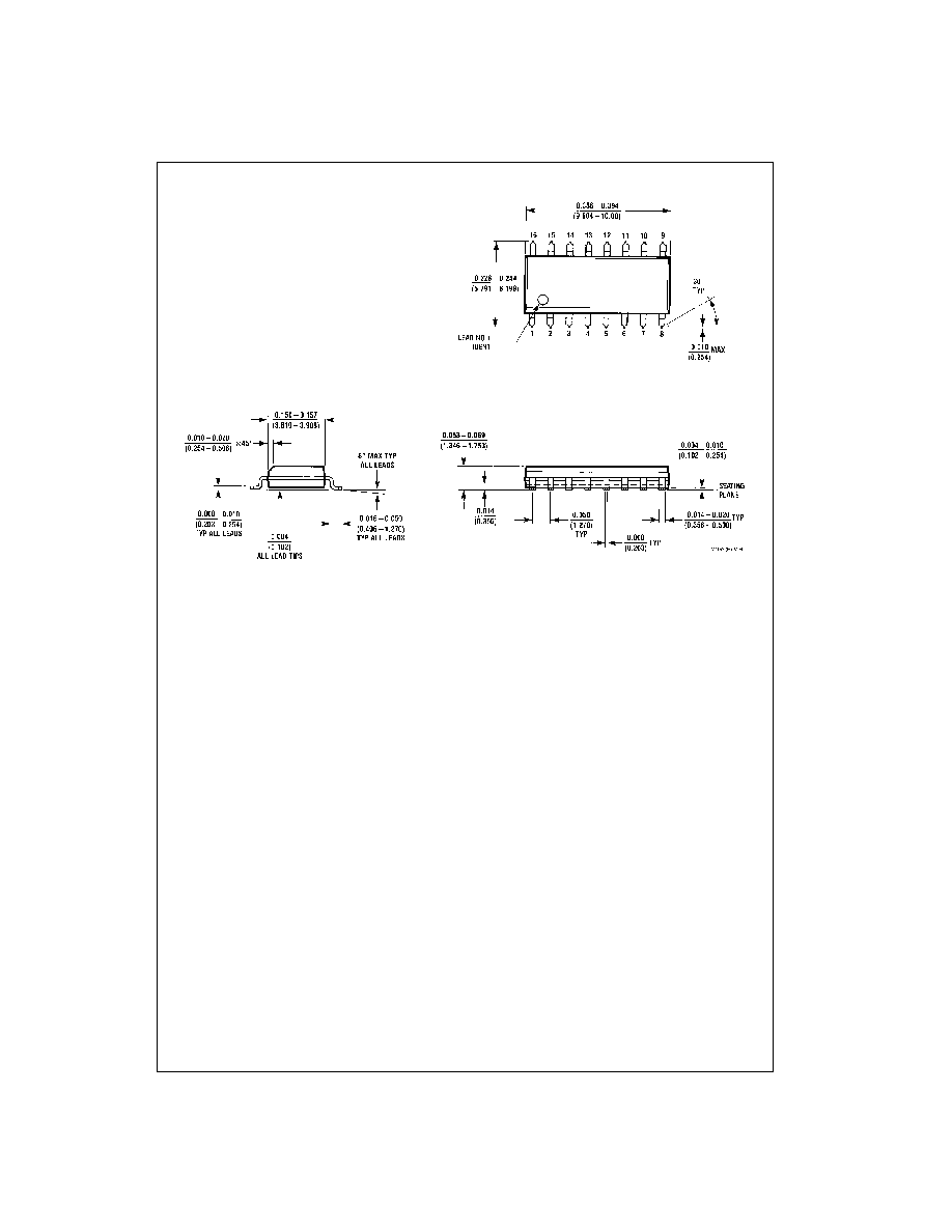
Physical Dimensions
inches (millimeters) unless otherwise noted
16-Lead (0.150' Wide) Molded Small Outline Package, JEDEC (S)
Package Number M16A
www.fairchildsemi.com
4
74F365 Hex B
u
f
f
e
r/
D
r
ive
r
wi
th 3-
S
T
A
T
E O
u
t
puts
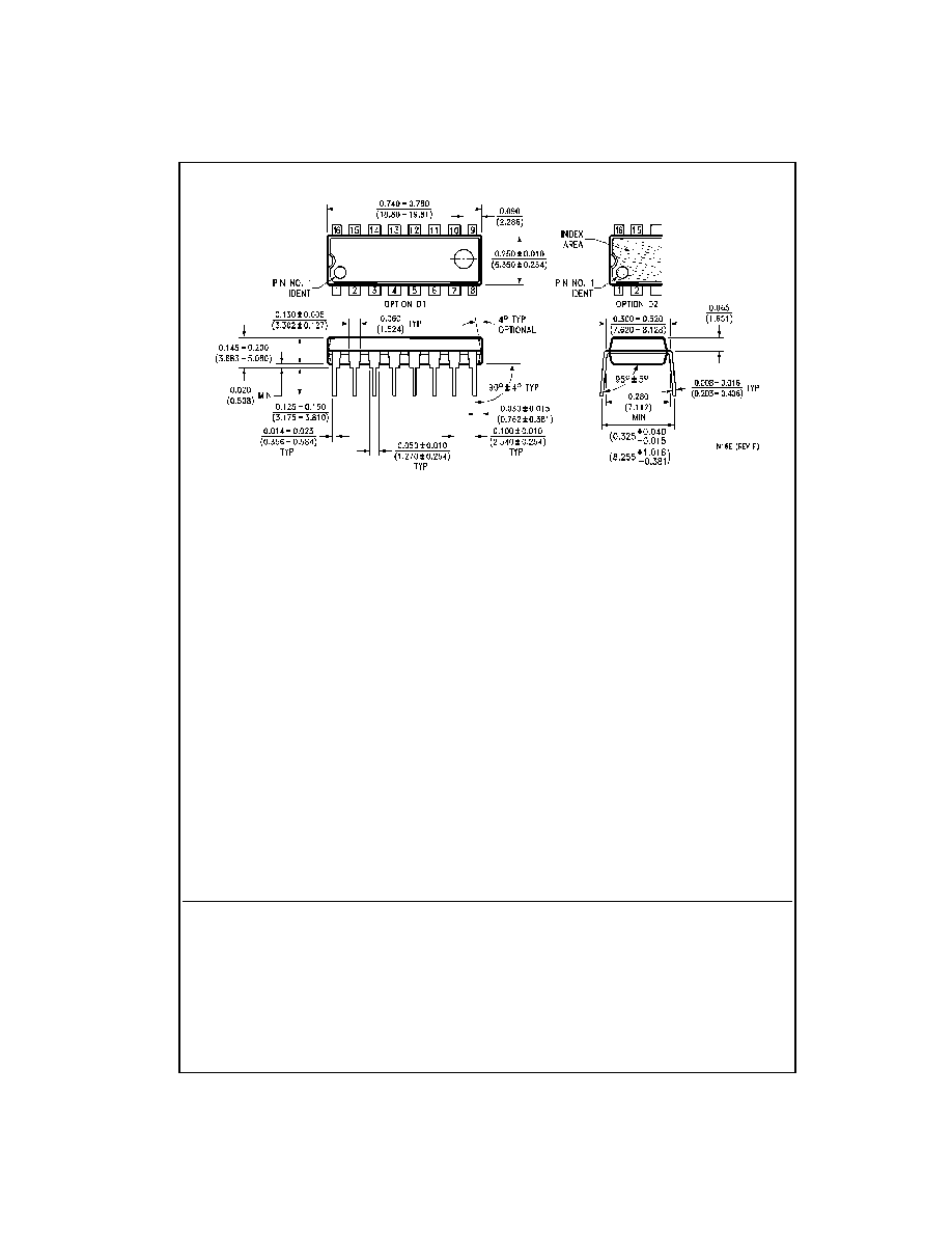
Physical Dimensions
inches (millimeters) unless otherwise noted (Continued)
16-Lead Plastic Dual-In-Line Package (PDIP), JEDEC MS-001, 0.300 Wide
Package Number N16E
Fairchild does not assume any responsibility for use of any circuitry described, no circuit patent licenses are implied and
Fairchild reserves the right at any time without notice to change said circuitry and specifications.
LIFE SUPPORT POLICY
FAIRCHILD'S PRODUCTS ARE NOT AUTHORIZED FOR USE AS CRITICAL COMPONENTS IN LIFE SUPPORT
DEVICES OR SYSTEMS WITHOUT THE EXPRESS WRITTEN APPROVAL OF THE PRESIDENT OF FAIRCHILD
SEMICONDUCTOR CORPORATION. As used herein:
1. Life support devices or systems are devices or systems
which, (a) are intended for surgical implant into the
body, or (b) support or sustain life, and (c) whose failure
to perform when properly used in accordance with
instructions for use provided in the labeling, can be rea-
sonably expected to result in a significant injury to the
user.
2. A critical component in any component of a life support
device or system whose failure to perform can be rea-
sonably expected to cause the failure of the life support
device or system, or to affect its safety or effectiveness.
www.fairchildsemi.com