 | –≠–ª–µ–∫—Ç—Ä–æ–Ω–Ω—ã–π –∫–æ–º–ø–æ–Ω–µ–Ω—Ç: 74F377PC | –°–∫–∞—á–∞—Ç—å:  PDF PDF  ZIP ZIP |

© 1999 Fairchild Semiconductor Corporation
DS009525
www.fairchildsemi.com
April 1988
Revised August 1999
7
4F377
O
c
t
a
l
D-T
ype
Fl
ip-
F
lo
p wit
h
C
l
ock
Enable
74F377
Octal D-Type Flip-Flop with Clock Enable
General Description
The 74F377 has eight edge-triggered, D-type flip-flops with
individual D inputs and Q outputs. The common buffered
Clock (CP) input loads all flip-flops simultaneously, when
the Clock Enable (CE) is LOW.
The register is fully edge-triggered. The state of each D
input, one setup time before the LOW-to-HIGH clock transi-
tion, is transferred to the corresponding flip-flop's Q output.
The CE input must be stable only one setup time prior to
the LOW-to-HIGH clock transition for predictable operation.
Features
s
Ideal for addressable register applications
s
Clock enable for address and data synchronization
applications
s
Eight edge-triggered D-type flip-flops
s
Buffered common clock
s
See 74F273 for master reset version
s
See 74F373 for transparent latch version
s
See 74F374 for 3-STATE version
Ordering Code:
Devices also available in Tape and Reel. Specify by appending the suffix letter "X" tot he ordering code.
Logic Symbols
IEEE/IEC
Connection Diagram
Order Number
Package Number
Package Description
74F377SC
M20B
20-Lead Small Outline Integrated Circuit (SOIC), JEDEC MS-013, 0.300 Wide
74F377SJ
M20D
20-Lead Small Outline Package (SOP), EIAJ TYPE II, 5.3mm Wide
74F377PC
N20A
20-Lead Plastic Dual-In-Line Package (PDIP), JEDEC MS-001, 0.300 Wide

www.fairchildsemi.com
2
74F377
Unit Loading/Fan Out
Mode Select-Function Table
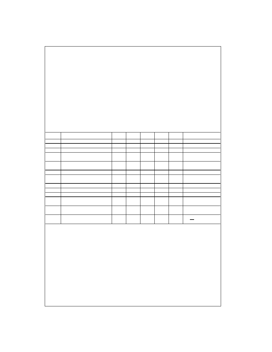
H
=
HIGH Voltage Level
h
=
HIGH Voltage Level one setup time prior to the LOW-to-HIGH Clock Transition
L
=
LOW Voltage Level
I
=
LOW Voltage Level one setup time prior to the LOW-to-HIGH Clock Transition
X
=
Immaterial
=
LOW-to-HIGH Clock Transition
Logic Diagram
Please note that this diagram is provided only for the understanding of logic operations and should not be used to estimate propagation delays.
Pin Names
Description
U.L.
Input I
IH
/I
IL
HIGH/LOW
Output I
OH
/I
OL
D
0
≠D
7
Data Inputs
1.0/1.0
20
µ
A/
-
0.6 mA
CE
Clock Enable (Active LOW)
1.0/1.0
20
µ
A/
-
0.6 mA
CP
Clock Pulse Input
1.0/1.0
20
µ
A/
-
0.6 mA
Q
0
≠Q
7
Data Outputs
50/33.3
-
1 mA/20 mA
Operating Mode
Inputs
Output
CP
CE
D
n
Q
n
Load "1"
I
h
H
Load "0"
I
I
L
Hold
h
X
No Change
(Do Nothing)
X
H
X
No Change
3
www.fairchildsemi.com
7
4F377
Absolute Maximum Ratings
(Note 1)
Recommended Operating
Conditions
Note 1: Absolute maximum ratings are values beyond which the device
may be damaged or have its useful life impaired. Functional operation
under these conditions is not implied.
Note 2: Either voltage limit or current limit is sufficient to protect inputs.
DC Electrical Characteristics
Storage Temperature
-
65
∞
C to
+
150
∞
C
Ambient Temperature under Bias
-
55
∞
C to
+
125
∞
C
Junction Temperature under Bias
-
55
∞
C to
+
150
∞
C
V
CC
Pin Potential to Ground Pin
-
0.5V to
+
7.0V
Input Voltage (Note 2)
-
0.5V to
+
7.0V
Input Current (Note 2)
-
30 mA to
+
5.0 mA
Voltage Applied to Output
in HIGH State (with V
CC
=
0V)
Standard Output
-
0.5V to V
CC
3-STATE Output
-
0.5V to
+
5.5V
Current Applied to Output
in LOW State (Max)
twice the rated I
OL
(mA)
ESD Last Passing Voltage (Min)
4000V
Free Air Ambient Temperature
0
∞
C to
+
70
∞
C
Supply Voltage
+
4.5V to
+
5.5V
Symbol
Parameter
Min
Typ
Max
Units
V
CC
Conditions
V
IH
Input HIGH Voltage
2.0
V
Recognized as a HIGH Signal
V
IL
Input LOW Voltage
0.8
V
Recognized as a LOW Signal
V
CD
Input Clamp Diode Voltage
-
1.2
V
Min
I
IN
=
-
18 mA
V
OH
Output HIGH
10% V
CC
2.5
V
Min
I
OH
=
-
1 mA
Voltage
5% V
CC
2.7
I
OH
=
-
1 mA
V
OL
Output LOW
10% V
CC
0.5
V
Min
I
OL
=
20 mA
Voltage
I
IH
Input HIGH Current
5.0
µ
A
Max
V
IN
=
2.7V
I
BVI
Input HIGH Current
7.0
µ
A
Max
V
IN
=
7.0V
Breakdown Test
I
IL
Input LOW Current
-
0.6
mA
Max
V
IN
=
0.5V
I
OS
Output Short-Circuit Current
-
60
-
150
mA
Max
V
OUT
=
0V
I
CEX
Output HIGH Leakage Current
50
µ
A
Max
V
OUT
=
V
CC
V
ID
Input Leakage
4.75
V
0.0
I
ID
=
1.9
µ
A
Test
All Other Pins Grounded
I
OD
Output Leakage
3.75
µ
A
0.0
V
IOD
=
150 mV
Circuit Current
All Other Pins Grounded
I
CCH
Power Supply Current
35
46
mA
Max
CP
=
I
CCL
44
56
D
n
=
MR
=
HIGH

www.fairchildsemi.com
4
74F377
AC Electrical Characteristics
AC Operating Requirements
Symbol
Parameter
T
A
=
+
25
∞
C
T
A
=
-
55
∞
C to
+
125
∞
C
T
A
=
0
∞
C to
+
70
∞
C
Units
V
CC
=
+
5.0V
V
CC
=
+
5.0V
V
CC
=
+
5.0V
C
L
=
50 pF
C
L
=
50 pF
C
L
=
50 pF
Min
Typ
Max
Min
Max
Min
Max
f
MAX
Maximum Clock Frequency
130
85
105
MHz
t
PLH
Propagation Delay
3.0
7.0
2.0
8.5
2.5
7.5
ns
t
PHL
CP to Q
n
4.0
9.0
3.0
10.5
3.5
9.0
Symbol
Parameter
T
A
=
+
25
∞
C
T
A
=
-
55
∞
C to
+
125
∞
C
T
A
=
0
∞
C to
+
70
∞
C
Units
V
CC
=
+
5.0V
V
CC
=
+
5.0V
V
CC
=
+
5.0V
Min
Max
Min
Max
Min
Max
t
S
(H)
Setup Time, HIGH or LOW
3.0
3.5
3.0
ns
t
S
(L)
D
n
to CP
3.5
4.0
3.5
t
H
(H)
Hold Time, HIGH or LOW
0.5
1.0
0.5
ns
t
H
(L)
D
n
to CP
1.0
1.0
1.0
t
S
(H)
Setup Time, HIGH or LOW
4.1
4.0
4.1
ns
t
S
(L)
CE to CP
3.5
5.0
4.0
t
H
(H)
Hold Time, HIGH to LOW
0.5
1.5
0.5
ns
t
H
(L)
CE to CP
2.0
2.5
2.0
t
W
(H)
Clock Pulse Width,
6.0
5.0
6.0
ns
t
W
(L)
HIGH or LOW
6.0
5.0
6.0

5
www.fairchildsemi.com
7
4F377
Physical Dimensions
inches (millimeters) unless otherwise noted
20-Lead Small Outline Integrated Circuit (SOIC), JEDEC MS-013, 0.300 Wide
Package Number M20B
20-Lead Small Outline Package (SOP), EIAJ TYPE II, 5.3mm Wide
Package Number M20D