 | –≠–ª–µ–∫—Ç—Ä–æ–Ω–Ω—ã–π –∫–æ–º–ø–æ–Ω–µ–Ω—Ç: 74F378SC | –°–∫–∞—á–∞—Ç—å:  PDF PDF  ZIP ZIP |
© 1999 Fairchild Semiconductor Corporation
DS009526
www.fairchildsemi.com
April 1988
Revised August 1999
7
4F378 P
a
ral
l
el
D-
T
ype
Regi
st
er w
i
th Enabl
e
74F378
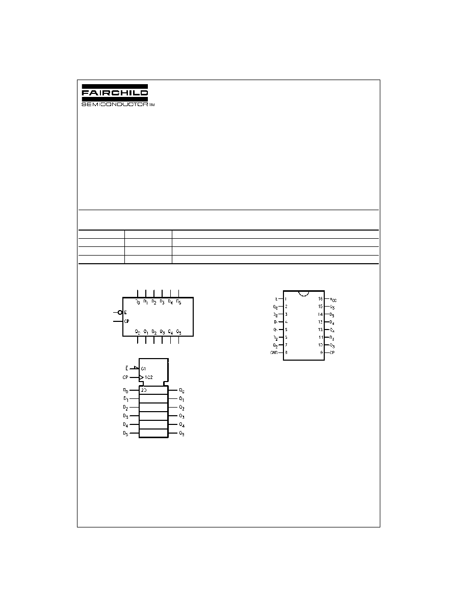
Parallel D-Type Register with Enable
General Description
The 74F378 is a 6-bit register with a buffered common
Enable. This device is similar to the 74F174, but with com-
mon Enable rather than common Master Reset.
Features
s
6-bit high-speed parallel register
s
Positive edge-triggered D-type inputs
s
Fully buffered common clock and enable inputs
s
Input clamp diodes limit high-speed termination effects
s
Full TTL and CMOS compatible
Ordering Code:
Devices also available in Tape and Reel. Specify by appending the suffix letter "X" to the ordering code.
Logic Symbols
IEEE/IEC
Connection Diagram
Order Number
Package Number
Package Description
74F378SC
M16A
16-Lead Small Outline Integrated Circuit (SOIC), JEDEC MS-012, 0.150 Narrow
74F378SJ
M16D
16-Lead Small Outline Package (SOP), EIAJ TYPE II, 5.3mm Wide
74F378PC
N16E
16-Lead Plastic Dual-In-Line Package (PDIP), JEDEC MS-001, 0.300 Wide
www.fairchildsemi.com
2
74F378
Unit Loading/Fan Out
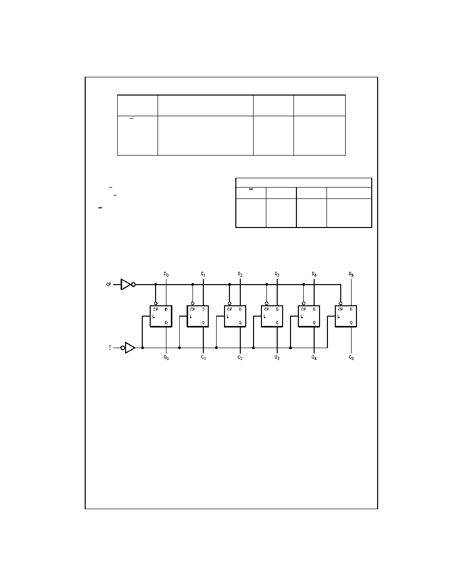
Functional Description
The 74F378 consists of six edge-triggered D-type flip-flops
with individual D inputs and Q inputs. The Clock (CP) and
Enable (E) inputs are common to all flip-flops.
When the E input is LOW, new data is entered into the reg-
ister on the LOW-to-HIGH transition of the CP input. When
the E input is HIGH the register will retain the present data
independent of the CP input.
Truth Table
H
=
HIGH Voltage Level
L
=
LOW Voltage Level
X
=
Immaterial
=
LOW-to-HIGH Clock Transition
Logic Diagram
Please note that this diagram is provided only for the understanding of logic operations and should not be used to estimate propagation delays.
Pin Names
Description
U.L.
Input I
IH
/I
IL
HIGH/LOW
Output I
OH
/I
OL
E
Enable Input (Active LOW)
1.0/1.0
20
µ
A/
-
0.6 mA
D
0
≠D
5
Data Inputs
1.0/1.0
20
µ
A/
-
0.6 mA
CP
Clock Pulse Input (Active Rising Edge)
1.0/1.0
20
µ
A/
-
0.6 mA
Q
0
≠Q
5
Outputs
50/33.3
-
1 mA/20 mA
Inputs
Output
E
CP
D
n
Q
n
H
X
No Change
L
H
H
L
L
L

3
www.fairchildsemi.com
7
4F378
Absolute Maximum Ratings
(Note 1)
Recommended Operating
Conditions
Note 1: Absolute maximum ratings are values beyond which the device
may be damaged or have its useful life impaired. Functional operation
under these conditions is not implied.
Note 2: Either voltage limit or current limit is sufficient to protect inputs.
DC Electrical Characteristics
Storage Temperature
-
65
∞
C to
+
150
∞
C
Ambient Temperature under Bias
-
55
∞
C to
+
125
∞
C
Junction Temperature under Bias
-
55
∞
C to
+
150
∞
C
V
CC
Pin Potential to Ground Pin
-
0.5V to
+
7.0V
Input Voltage (Note 2)
-
0.5V to
+
7.0V
Input Current (Note 2)
-
30 mA to
+
5.0 mA
Voltage Applied to Output
in HIGH State (with V
CC
=
0V)
Standard Output
-
0.5V to V
CC
3-STATE Output
-
0.5V to
+
5.5V
Current Applied to Output
in LOW State (Max)
twice the rated I
OL
(mA)
Free Air Ambient Temperature
0
∞
C to
+
70
∞
C
Supply Voltage
+
4.5V to
+
5.5V
Symbol
Parameter
Min
Typ
Max
Units
V
CC
Conditions
V
IH
Input HIGH Voltage
2.0
V
Recognized as a HIGH Signal
V
IL
Input LOW Voltage
0.8
V
Recognized as a LOW Signal
V
CD
Input Clamp Diode Voltage
-
1.2
V
Min
I
IN
=
-
18 mA
V
OH
Output HIGH
10% V
CC
2.5
V
Min
I
OH
=
-
1 mA
Voltage
5% V
CC
2.7
I
OH
=
-
1 mA
V
OL
Output LOW
10% V
CC
0.5
V
Min
I
OL
=
20 mA
Voltage
I
IH
Input HIGH
5.0
µ
A
Max
V
IN
=
2.7V
Current
I
BVI
Input HIGH Current
7.0
µ
A
Max
V
IN
=
7.0V
Breakdown Test
I
CEX
Output HIGH
50
µ
A
Max
V
OUT
=
V
CC
Leakage Current
V
ID
Input Leakage
4.75
V
0.0
I
ID
=
1.9
µ
A
Test
All Other Pins Grounded
I
OD
Output Leakage
3.75
µ
A
0.0
V
IOD
=
150 mV
Circuit Current
All Other Pins Grounded
I
IL
Input LOW Current
-
0.6
mA
Max
V
IN
=
0.5V
I
OS
Output Short-Circuit Current
-
60
-
150
mA
Max
V
OUT
=
0V
I
CCL
Power Supply Current
30
45
mA
Max
V
O
=
LOW
www.fairchildsemi.com
4
74F378
AC Electrical Characteristics
AC Operating Requirements
Symbol
Parameter
T
A
=
+
25
∞
C
T
A
=
-
55
∞
C to
+
125
∞
C
T
A
=
0
∞
C to
+
70
∞
C
Units
V
CC
=
+
5.0V
V
CC
=
+
5.0V
V
CC
=
+
5.0V
C
L
=
50 pF
C
L
=
50 pF
C
L
=
50 pF
Min
Typ
Max
Min
Max
Min
Max
f
MAX
Maximum Input Frequency
80
100
70
80
MHz
t
PLH
Propagation Delay
3.0
5.5
7.5
3.0
10.0
3.0
8.5
ns
t
PHL
CP to Q
n
3.5
6.0
8.5
3.5
10.5
3.5
9.5
Symbol
Parameter
T
A
=
+
25
∞
C
T
A
=
-
55
∞
C to
+
125
∞
C
T
A
=
0
∞
C to
+
70
∞
C
Units
V
CC
=
+
5.0V
V
CC
=
+
5.0V
V
CC
=
+
5.0V
Min
Max
Min
Max
Min
Max
t
S
(H)
Setup Time, HIGH or LOW
4.0
5.0
4.0
ns
t
S
(L)
D
n
to CP
4.0
5.0
4.0
t
H
(H)
Hold Time, HIGH or LOW
0
2.0
0
t
H
(L)
D
n
to CP
0
2.0
0
t
S
(H)
Setup Time, HIGH or LOW
6.0
4.5
6.0
ns
t
S
(L)
E to CP
10.0
13.0
10.0
t
H
(H)
Hold Time, HIGH or LOW
0
0
0
t
H
(L)
E to CP
0
0
0
t
W
(H)
CP Pulse Width
4.0
5.0
4.0
ns
t
W
(L)
HIGH or LOW
6.0
7.5
6.0
5
www.fairchildsemi.com
7
4F378
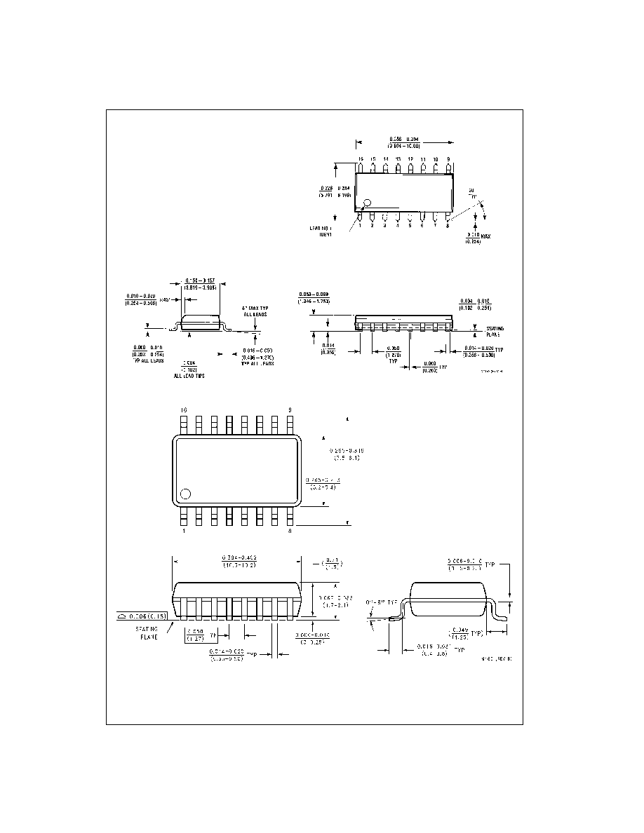
Physical Dimensions
inches (millimeters) unless otherwise noted
16-Lead Small Outline Integrated Circuit (SOIC), JEDEC MS-012, 0.150 Narrow
Package Number M16A
16-Lead Small Outline Package (SOP), EIAJ TYPE II, 5.3mm Wide
Package Number M16D