 | –≠–ª–µ–∫—Ç—Ä–æ–Ω–Ω—ã–π –∫–æ–º–ø–æ–Ω–µ–Ω—Ç: 74F379SC | –°–∫–∞—á–∞—Ç—å:  PDF PDF  ZIP ZIP |
© 1999 Fairchild Semiconductor Corporation
DS009527
www.fairchildsemi.com
May 1988
Revised August 1999
7
4F379 Q
uad Para
ll
el Regis
t
er
wit
h
Ena
b
le
74F379
Quad Parallel Register with Enable
General Description
The 74F379 is a 4-bit register with buffered common
Enable. This device is similar to the 74F175 but features
the common Enable rather than common Master Reset.
Features
s
Edge triggered D-type inputs
s
Buffered positive edge-triggered clock
s
Buffered common enable input
s
True and complement outputs
Ordering Code:
Devices also available in Tape and Reel. Specify by appending the suffix letter "X" to the ordering code.
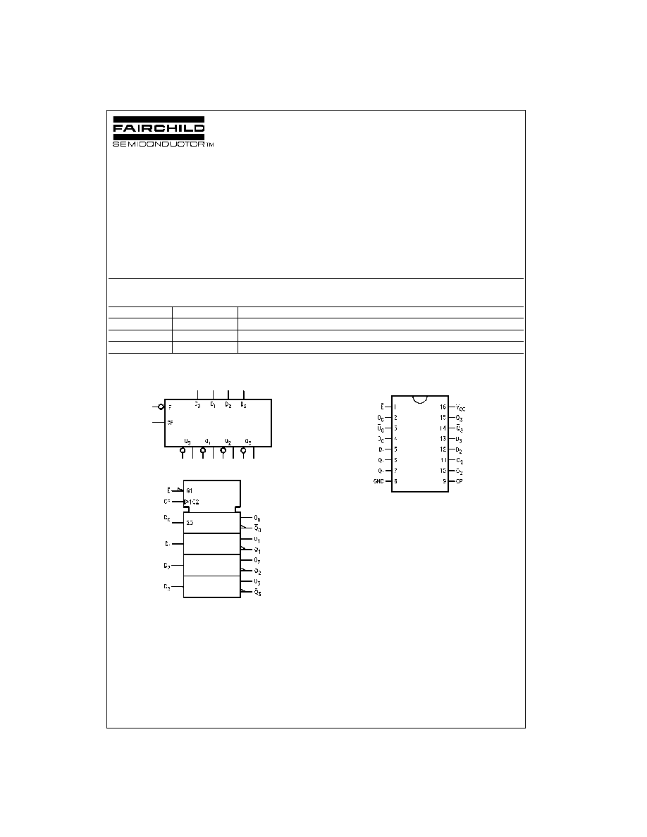
Logic Symbols
IEEE/IEC
Connection Diagram
Order Number
Package Number
Package Description
74F379SC
M16A
16-Lead Small Outline Integrated Circuit (SOIC), JEDEC MS-012, 0.150 Narrow
74F379SJ
M16D
16-Lead Small Outline Package (SOP), EIAJ TYPE II, 5.3mm Wide
74F379PC
N16E
16-Lead Plastic Dual-In-Line Package (PDIP), JEDEC MS-001, 0.300 Wide

www.fairchildsemi.com
2
74F379
Unit Loading/Fan Out
Functional Description
The 74F379 consists of four edge-triggered D-type flip-
flops with individual D inputs and Q and Q outputs. The
Clock (CP) and Enable (E) inputs are common to all flip-
flops. When the E is input HIGH, the register will retain the
present data independent of the CP input. The D
n
and E
inputs can change when the clock is in either state, pro-
vided that the recommended setup and hold times are
observed.
Truth Table
H
=
HIGH Voltage Level
L
=
LOW Voltage Level
X
=
Immaterial
=
LOW-to-HIGH Transition
NC
=
No Change
Logic Diagram
Please note that this diagram is provided only for the understanding of logic operations and should not be used to estimate propagation delays.
Pin Names
Description
U.L.
Input I
IH
/I
IL
HIGH/LOW
Output I
OH
/I
OL
E
Enable Input (Active LOW)
1.0/1.0
20
µ
A/
-
0.6 mA
D
0
≠D
3
Data Inputs
1.0/1.0
20
µ
A/
-
0.6 mA
CP
Clock Pulse Input (Active Rising Edge)
1.0/1.0
20
µ
A/
-
0.6 mA
Q
0
≠Q
3
Flip-Flop Outputs
50/33.3
-
1 mA/20 mA
Q
0
≠Q
3
Complement Outputs
50/33.3
-
1 mA/20 mA
Inputs
Outputs
E
CP
D
n
Q
n
Q
n
H
X
NC
NC
L
H
H
L
L
L
L
H
3
www.fairchildsemi.com
7
4F379
Absolute Maximum Ratings
(Note 1)
Recommended Operating
Conditions
Note 1: Absolute maximum ratings are values beyond which the device
may be damaged or have its useful life impaired. Functional operation
under these conditions is not implied.
Note 2: Either voltage limit or current limit is sufficient to protect inputs.
DC Electrical Characteristics
Storage Temperature
-
65
∞
C to
+
150
∞
C
Ambient Temperature under Bias
-
55
∞
C to
+
125
∞
C
Junction Temperature under Bias
-
55
∞
C to
+
150
∞
C
V
CC
Pin Potential to Ground Pin
-
0.5V to
+
7.0V
Input Voltage (Note 2)
-
0.5V to
+
7.0V
Input Current (Note 2)
-
30 mA to
+
5.0 mA
Voltage Applied to Output
in HIGH State (with V
CC
=
0V)
Standard Output
-
0.5V to V
CC
3-STATE Output
-
0.5V to
+
5.5V
Current Applied to Output
in LOW State (Max)
twice the rated I
OL
(mA)
ESD Last Passing Voltage (Min)
4000V
Free Air Ambient Temperature
0
∞
C to
+
70
∞
C
Supply Voltage
+
4.5V to
+
5.5V
Symbol
Parameter
Min
Typ
Max
Units
V
CC
Conditions
V
IH
Input HIGH Voltage
2.0
V
Recognized as a HIGH Signal
V
IL
Input LOW Voltage
0.8
V
Recognized as a LOW Signal
V
CD
Input Clamp Diode Voltage
-
1.2
V
Min
I
IN
=
-
18 mA
V
OH
Output HIGH
10% V
CC
2.5
V
Min
I
OH
=
-
1 mA
Voltage
5% V
CC
2.7
I
OH
=
-
1 mA
V
OL
Output LOW
10% V
CC
0.5
V
Min
I
OL
=
20 mA
Voltage
I
IH
Input HIGH
5.0
µ
A
Max
V
IN
=
2.7V
Current
I
BVI
Input HIGH Current
7.0
µ
A
Max
V
IN
=
7.0V
Breakdown Test
I
CEX
Output HIGH
50
µ
A
Max
V
OUT
=
V
CC
Leakage Current
V
ID
Input Leakage
4.75
V
0.0
I
ID
=
1.9
µ
A
Test
All Other Pins Grounded
I
OD
Output Leakage
3.75
µ
A
0.0
V
IOD
=
150 mV
Circuit Current
All Other Pins Grounded
I
IL
Input LOW Current
-
0.6
mA
Max
V
IN
=
0.5V
I
OS
Output Short-Circuit Current
-
60
-
150
mA
Max
V
OUT
=
0V
I
CCL
Power Supply Current
28
40
mA
Max
V
O
=
LOW
www.fairchildsemi.com
4
74F379
AC Electrical Characteristics
AC Operating Requirements
Symbol
Parameter
T
A
=
+
25
∞
C
T
A
=
-
55
∞
C to
+
125
∞
C
T
A
=
0
∞
C to
+
70
∞
C
Units
V
CC
=
+
5.0V
V
CC
=
+
5.0V
V
CC
=
+
5.0V
C
L
=
50 pF
C
L
=
50 pF
C
L
=
50 pF
Min
Typ
Max
Min
Max
Min
Max
f
MAX
Maximum Clock Frequency
100
140
75
100
MHz
t
PLH
Propagation Delay
3.5
5.0
6.5
3.0
8.5
3.5
7.5
ns
t
PHL
CP to Q
n
, Q
n
5.0
6.5
8.5
4.0
10.0
5.0
9.5
Symbol
Parameter
T
A
=
+
25
∞
C
T
A
=
-
55
∞
C to
+
125
∞
C
T
A
=
0
∞
C to
+
70
∞
C
Units
V
CC
=
+
5.0V
V
CC
=
+
5.0V
V
CC
=
+
5.0V
Min
Max
Min
Max
Min
Max
t
S
(H)
Setup Time, HIGH or LOW
3.0
4.0
3.0
ns
t
S
(L)
D
n
to CP
3.0
4.0
3.0
t
H
(H)
Hold Time, HIGH or LOW
1.0
2.0
1.0
t
H
(L)
D
n
to CP
1.0
2.0
1.0
t
S
(H)
Setup Time, HIGH or LOW
6.0
8.0
6.0
ns
t
S
(L)
E to CP
6.0
8.0
6.0
t
H
(H)
Hold Time, HIGH or LOW
0
0
0
t
H
(L)
E to CP
0
0
0
t
W
(H)
CP Pulse Width
4.0
5.0
4.0
ns
t
W
(L)
HIGH or LOW
5.0
7.0
5.0
5
www.fairchildsemi.com
7
4F379
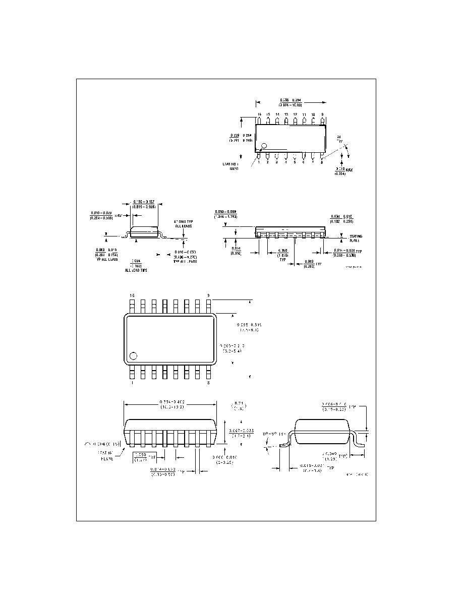
Physical Dimensions
inches (millimeters) unless otherwise noted
16-Lead Small Outline Integrated Circuit (SOIC), JEDEC MS-012, 0.150 Narrow
Package Number M16A
16-Lead Small Outline Package (SOP), EIAJ TYPE II, 5.3mm Wide
Package Number M16D
www.fairchildsemi.com
6
74F379
Quad Par
a
ll
el
Regi
ster
wi
th
Enable
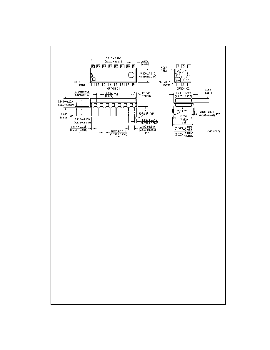
Physical Dimensions
inches (millimeters) unless otherwise noted (Continued)
16-Lead Plastic Dual-In-Line Package (PDIP), JEDEC MS-001, 0.300 Wide
Package Number N16E
Fairchild does not assume any responsibility for use of any circuitry described, no circuit patent licenses are implied and
Fairchild reserves the right at any time without notice to change said circuitry and specifications.
LIFE SUPPORT POLICY
FAIRCHILD'S PRODUCTS ARE NOT AUTHORIZED FOR USE AS CRITICAL COMPONENTS IN LIFE SUPPORT
DEVICES OR SYSTEMS WITHOUT THE EXPRESS WRITTEN APPROVAL OF THE PRESIDENT OF FAIRCHILD
SEMICONDUCTOR CORPORATION. As used herein:
1. Life support devices or systems are devices or systems
which, (a) are intended for surgical implant into the
body, or (b) support or sustain life, and (c) whose failure
to perform when properly used in accordance with
instructions for use provided in the labeling, can be rea-
sonably expected to result in a significant injury to the
user.
2. A critical component in any component of a life support
device or system whose failure to perform can be rea-
sonably expected to cause the failure of the life support
device or system, or to affect its safety or effectiveness.
www.fairchildsemi.com