 | –≠–ª–µ–∫—Ç—Ä–æ–Ω–Ω—ã–π –∫–æ–º–ø–æ–Ω–µ–Ω—Ç: 74F382PC | –°–∫–∞—á–∞—Ç—å:  PDF PDF  ZIP ZIP |
© 1999 Fairchild Semiconductor Corporation
DS009529
www.fairchildsemi.com
May 1988
Revised August 1999
7
4F382 4-Bi
t Arit
hmeti
c
Lo
gic Unit
74F382
4-Bit Arithmetic Logic Unit
General Description
The 74F382 performs three arithmetic and three logic oper-
ations on two 4-bit words, A and B. Two additional Select
input codes force the Function outputs LOW or HIGH. An
Overflow output is provided for convenience in twos com-
plement arithmetic. A Carry output is provided for ripple
expansion. For high-speed expansion using a Carry Looka-
head Generator, refer to the 74F381 data sheet.
Features
s
Performs six arithmetic and logic functions
s
Selectable LOW (clear) and HIGH (preset) functions
s
LOW input loading minimizes drive requirements
s
Carry output for ripple expansion
s
Overflow output for twos complement arithmetic
Ordering Code:
Devices also available in Tape and Reel. Specify by appending the suffix letter "X" to the ordering code.
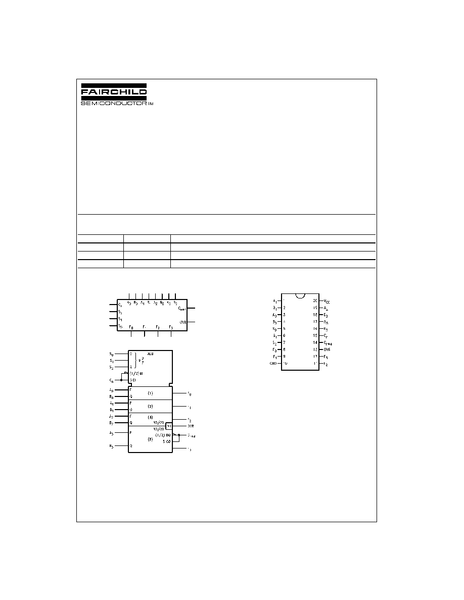
Logic Symbols
IEEE/IEC
Connection Diagram
Order Number
Package Number
Package Description
74F382SC
M20B
20-Lead Small Outline Integrated Circuit (SOIC), JEDEC MS-013, 0.300 Wide
74F382SJ
M20D
20-Lead Small Outline Package (SOP), EIAJ TYPE II, 5.3mm Wide
74F382PC
N20A
20-Lead Plastic Dual-In-Line Package (PDIP), JEDEC MS-001, 0.300 Wide
www.fairchildsemi.com
2
74F382
Unit Loading/Fan Out
Functional Description
Signals applied to the Select inputs S
0
≠S
2
determine the
mode of operation, as indicated in the Function Select
Table. An extensive listing of input and output levels is
shown in the Truth Table. The circuit performs the arith-
metic functions for either active HIGH or active LOW oper-
ands, with output levels in the same convention. In the
Subtract operating modes, it is necessary to force a carry
(HIGH for active HIGH operands, LOW for active LOW
operands) into the C
n
input of the least significant package.
Ripple expansion is illustrated in Figure 2. The overflow
output OVR is the Exclusive-OR of C
n
+
3
and C
n
+
4
; a
HIGH signal on OVR indicates overflow in twos comple-
ment operation. Typical delays for Figure 2 are given in
Figure 1.
Function Select Table
H
=
HIGH Voltage Level
L
=
LOW Voltage Level
FIGURE 1. 16-Bit Delay Tabulation
FIGURE 2. 16-Bit Ripply Carry ALU Expansion
Pin Names
Description
U.L.
Input I
IH
/I
IL
HIGH/LOW
Output I
OH
/I
OL
A
0
≠A
3
A Operand Inputs
1.0/4.0
20
µ
A/
-
2.4 mA
B
0
≠B
3
B Operand Inputs
1.0/4.0
20
µ
A/
-
2.4 mA
S
0
≠S
2
Function Select Inputs
1.0/1.0
20
µ
A/
-
0.6 mA
C
n
Carry Input
1.0/5.0
20
µ
A/
-
3.0 mA
C
n
+
4
Carry Output
50/33.3
-
1 mA/20 mA
OVR
Overflow Output
50/33.3
-
1 mA/20 mA
F
0
≠F
3
Function Outputs
50/33.3
-
1 mA/20 mA
Select
Operation
S
0
S
1
S
2
L
L
L
Clear
H
L
L
B Minus A
L
H
L
A Minus B
H
H
L
A Plus B
L
L
H
A
B
H
L
H
A
+
B
L
H
H
AB
H
H
H
Preset
Path Segment
Toward
Output
F
C
n
+
4
, OVR
A
1
or B
1
to C
n
+
4
6.5 ns
6.5 ns
C
n
to C
n
+
4
6.3 ns
6.3 ns
C
n
to C
n
+
4
6.3 ns
6.3 ns
C
n
to F
8.1 ns
--
C
n
to C
n
+
4
, OVR
--
8.0 ns
Total Delay
27.2 ns
27.1 ns
3
www.fairchildsemi.com
7
4F382
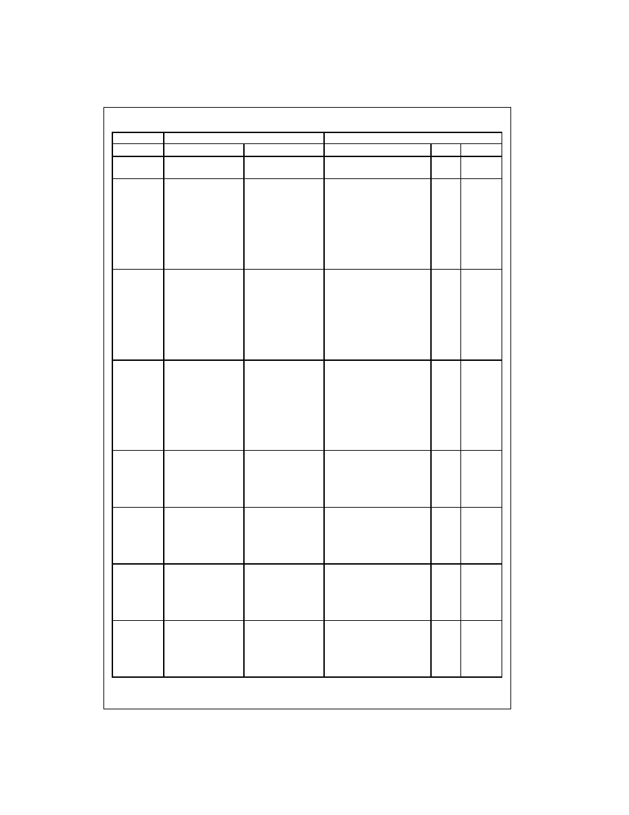
Truth Table
H
=
HIGH Voltage Level
L
=
LOW Voltage Level
X
=
Immaterial
Inputs
Outputs
Function
S
0
S
1
S
2
C
n
A
n
B
n
F
0
F
1
F
2
F
3
OVR
C
n
+
4
CLEAR
L
L
L
L
X
X
L
L
L
L
H
H
H
X
X
L
L
L
L
H
H
B MINUS A
H
L
L
L
L
L
H
H
H
H
L
L
L
L
H
L
H
H
H
L
H
L
H
L
L
L
L
L
L
L
L
H
H
H
H
H
H
L
L
H
L
L
L
L
L
L
L
H
H
L
H
H
H
H
H
L
H
H
H
L
H
L
L
L
L
L
H
H
H
L
L
L
L
L
H
A MINUS B
L
H
L
L
L
L
H
H
H
H
L
L
L
L
H
L
L
L
L
L
L
L
H
L
L
H
H
H
L
H
L
H
H
H
H
H
H
L
L
H
L
L
L
L
L
L
L
H
H
L
H
H
L
L
L
L
L
H
H
L
H
H
H
H
L
H
H
H
H
L
L
L
L
L
H
A PLUS B
H
H
L
L
L
L
L
L
L
L
L
L
L
L
H
H
H
H
H
L
L
L
H
L
H
H
H
H
L
L
L
H
H
L
H
H
H
L
H
H
L
L
H
L
L
L
L
L
H
L
H
L
L
L
L
L
H
H
H
L
L
L
L
L
L
H
H
H
H
H
H
H
H
L
H
A
B
L
L
H
X
L
L
L
L
L
L
L
L
X
L
H
H
H
H
H
L
L
L
H
L
H
H
H
H
L
L
X
H
H
L
L
L
L
H
H
H
H
L
H
H
H
H
H
H
A
+
B
H
L
H
X
L
L
L
L
L
L
L
L
X
L
H
H
H
H
H
L
L
X
H
L
H
H
H
H
L
L
L
H
H
H
H
H
H
L
L
H
H
H
H
H
H
H
H
H
AB
L
H
H
X
L
L
L
L
L
L
H
H
X
L
H
L
L
L
L
L
L
X
H
L
L
L
L
L
H
H
L
H
H
H
H
H
H
L
L
H
H
H
H
H
H
H
H
H
PRESET
H
H
H
X
L
L
H
H
H
H
L
L
X
L
H
H
H
H
H
L
L
X
H
L
H
H
H
H
L
L
L
H
H
H
H
H
H
L
L
H
H
H
H
H
H
H
H
H
www.fairchildsemi.com
4
74F382
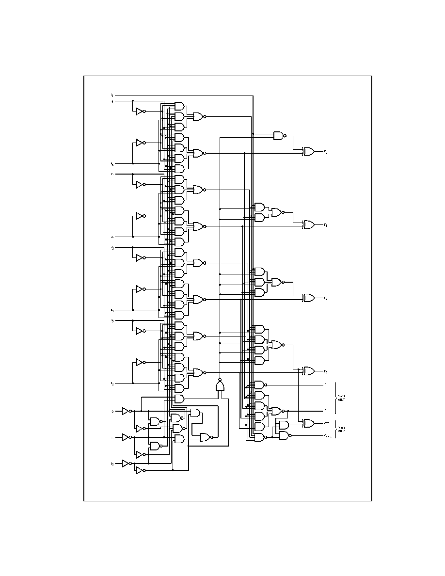
Logic Diagram
Please note that this diagram is provided only for the understanding of logic operations and should not be used to estimate propagation delays.
5
www.fairchildsemi.com
7
4F382
Absolute Maximum Ratings
(Note 1)
Recommended Operating
Conditions
Note 1: Absolute maximum ratings are values beyond which the device
may be damaged or have its useful life impaired. Functional operation
under these conditions is not implied.
Note 2: Either voltage limit or current limit is sufficient to protect inputs.
DC Electrical Characteristics
over Operating Temperature Range unless otherwise specified
Storage Temperature
-
65
∞
C to
+
150
∞
C
Ambient Temperature under Bias
-
55
∞
C to
+
125
∞
C
Junction Temperature under Bias
-
55
∞
C to
+
150
∞
C
V
CC
Pin Potential to Ground Pin
-
0.5V to
+
7.0V
Input Voltage (Note 2)
-
0.5V to
+
7.0V
Input Current (Note 2)
-
30 mA to
+
5.0 mA
Voltage Applied to Output
in HIGH State (with V
CC
=
0V)
Standard Output
-
0.5V to V
CC
3-STATE Output
-
0.5V to
+
5.5V
Current Applied to Output
in LOW State (Max)
twice the rated I
OL
(mA)
Free Air Ambient Temperature
0
∞
C to
+
70
∞
C
Supply Voltage
+
4.5V to
+
5.5V
Symbol
Parameter
Min
Typ
Max
Units
V
CC
Conditions
V
IH
Input HIGH Voltage
2.0
V
Recognized as a HIGH Signal
V
IL
Input LOW Voltage
0.8
V
Recognized as a LOW Signal
V
CD
Input Clamp Diode Voltage
-
1.2
V
Min
I
IN
=
-
18 mA
V
OH
Output HIGH
10% V
CC
2.5
V
Min
I
OH
=
-
1 mA
Voltage
5% V
CC
2.7
I
OH
=
-
1 mA
V
OL
Output LOW
10% V
CC
0.5
V
Min
I
OL
=
20 mA
Voltage
I
IH
Input HIGH
5.0
µ
A
Max
V
IN
=
2.7V
Current
I
BVI
Input HIGH Current
7.0
µ
A
Max
V
IN
=
7.0V
Breakdown Test
I
CEX
Output HIGH
50
µ
A
Max
V
OUT
=
V
CC
Leakage Current
V
ID
Input Leakage
4.75
V
0.0
I
ID
=
1.9
µ
A
Test
All Other Pins Grounded
I
OD
Output Leakage
3.75
µ
A
0.0
V
IOD
=
150 mV
Circuit Current
All Other Pins Grounded
I
IL
Input LOW Current
-
0.6
V
IN
=
0.5V (S
0
≠ S
2
)
-
2.4
mA
Max
V
IN
=
0.5V (A
0
≠ A
3
, B
0
≠ B
3
)
-
3.0
V
IN
=
0.5V (C
n
)
I
OS
Output Short-Circuit Current
-
60
-
150
mA
Max
V
OUT
=
0V
I
CC
Power Supply Current
54
81
mA
Max
www.fairchildsemi.com
6
74F382
AC Electrical Characteristics
Symbol
Parameter
T
A
=
+
25
∞
C
T
A
=
0
∞
C to
+
70
∞
C
Units
V
CC
=
+
5.0V
V
CC
=
+
5.0V
C
L
=
50 pF
C
L
=
50 pF
Min
Typ
Max
Min
Max
t
PLH
Propagation Delay
3.0
8.1
12.0
3.0
13.0
ns
t
PHL
C
n
to F
i
2.5
5.7
8.0
2.5
9.0
t
PLH
Propagation Delay
4.0
10.4
15.0
3.5
17.0
ns
t
PHL
Any A or B to Any F
3.0
8.2
11.0
2.5
12.0
t
PLH
Propagation Delay
6.5
11.0
20.5
5.5
21.5
ns
t
PHL
S
i
to F
i
4.0
8.2
15.0
4.0
17.5
t
PLH
Propagation Delay
3.5
6.0
8.5
3.5
11.0
ns
t
PHL
A
i
or B
i
to C
n
+
4
3.5
6.5
9.0
3.5
10.5
t
PLH
Propagation Delay
7.0
12.5
16.5
7.0
17.5
ns
t
PHL
S
i
to OVR or C
n
+
4
5.0
9.0
12.0
5.0
14.5
t
PLH
Propagation Delay
2.5
5.6
8.0
2.0
9.0
ns
t
PHL
C
n
to C
n
+
4
3.5
6.3
9.0
2.0
10.0
t
PLH
Propagation Delay
3.5
8.0
11.0
3.5
13.0
ns
t
PHL
C
n
to OVR
2.5
7.1
10.0
2.5
11.0
t
PLH
Propagation Delay
7.0
11.5
15.5
7.0
16.5
ns
t
PHL
A
i
or B
i
to OVR
3.0
8.0
10.5
3.0
11.5
7
www.fairchildsemi.com
7
4F382
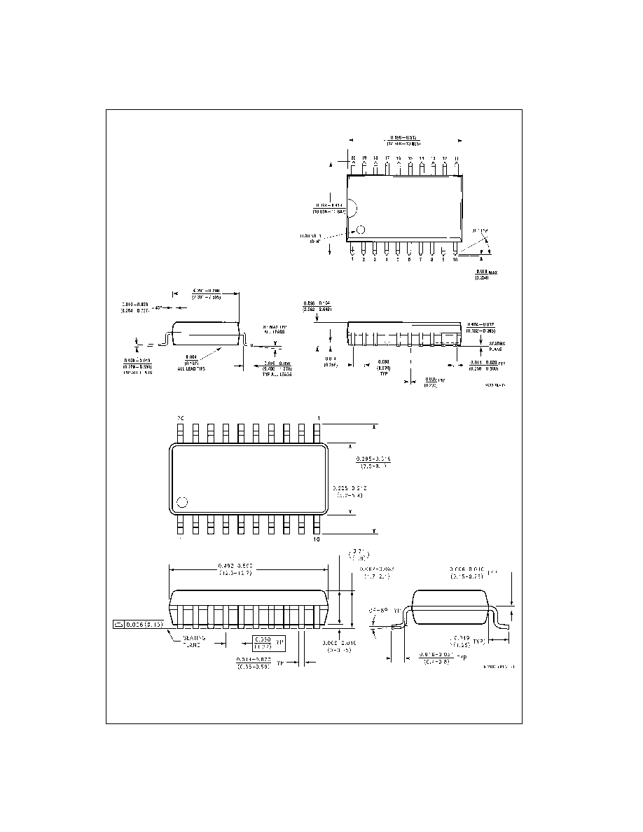
Physical Dimensions
inches (millimeters) unless otherwise noted
20-Lead Small Outline Integrated Circuit (SOIC), JEDEC MS-013, 0.300 Wide
Package Number M20B
20-Lead Small Outline Package (SOP), EIAJ TYPE II, 5.3mm Wide
Package Number M20D
www.fairchildsemi.com
8
74F3
82 4-
Bit
Ar
it
hm
et
i
c
Logi
c
U
n
it
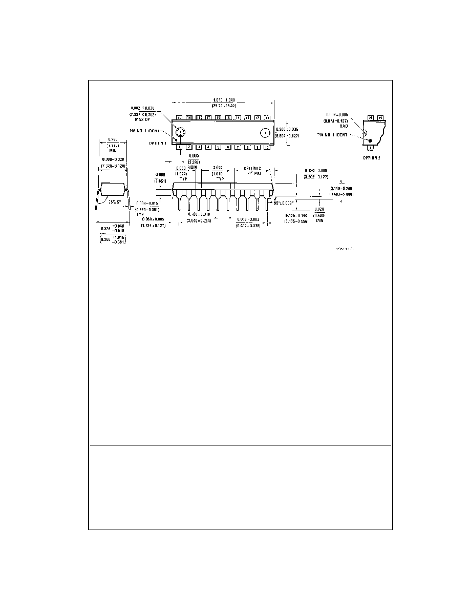
Physical Dimensions
inches (millimeters) unless otherwise noted (Continued)
20-Lead Plastic Dual-In-Line Package (PDIP), JEDEC MS-001, 0.300 Wide
Package Number N20A
Fairchild does not assume any responsibility for use of any circuitry described, no circuit patent licenses are implied and
Fairchild reserves the right at any time without notice to change said circuitry and specifications.
LIFE SUPPORT POLICY
FAIRCHILD'S PRODUCTS ARE NOT AUTHORIZED FOR USE AS CRITICAL COMPONENTS IN LIFE SUPPORT
DEVICES OR SYSTEMS WITHOUT THE EXPRESS WRITTEN APPROVAL OF THE PRESIDENT OF FAIRCHILD
SEMICONDUCTOR CORPORATION. As used herein:
1. Life support devices or systems are devices or systems
which, (a) are intended for surgical implant into the
body, or (b) support or sustain life, and (c) whose failure
to perform when properly used in accordance with
instructions for use provided in the labeling, can be rea-
sonably expected to result in a significant injury to the
user.
2. A critical component in any component of a life support
device or system whose failure to perform can be rea-
sonably expected to cause the failure of the life support
device or system, or to affect its safety or effectiveness.
www.fairchildsemi.com