 | –≠–ª–µ–∫—Ç—Ä–æ–Ω–Ω—ã–π –∫–æ–º–ø–æ–Ω–µ–Ω—Ç: 74F402PC | –°–∫–∞—á–∞—Ç—å:  PDF PDF  ZIP ZIP |
© 1999 Fairchild Semiconductor Corporation
DS009535
www.fairchildsemi.com
April 1988
Revised August 1999
7
4F402 S
e
ria
l
Data Polyno
m
i
al Generat
or/
C
hecker
74F402
Serial Data Polynomial Generator/Checker
General Description
The 74F402 expandable Serial Data Polynomial generator/
checker is an expandable version of the 74F401. It pro-
vides an advanced tool for the implementation of the most
widely used error detection scheme in serial digital han-
dling systems. A 4-bit control input selects one-of-six gen-
erator polynomials. The list of polynomials includes CRC-
16, CRC-CCITT and Ethernet
Æ
, as well as three other
standard polynomials (56
th
order, 48
th
order, 32
nd
order).
Individual clear and preset inputs are provided for floppy
disk and other applications. The Error output indicates
whether or not a transmission error has occurred. The
CWG Control input inhibits feedback during check word
transmission. The 74F402 is compatible with FAST
Æ
devices and with all TTL families.
Features
s
Guaranteed 30 MHz data rate
s
Six selectable polynomials
s
Other polynomials available
s
Separate preset and clear controls
s
Expandable
s
Automatic right justification
s
Error output open collector
s
Typical applications: Floppy and other disk storage sys-
tems Digital cassette and cartridge systems Data com-
munication systems
Ordering Code:
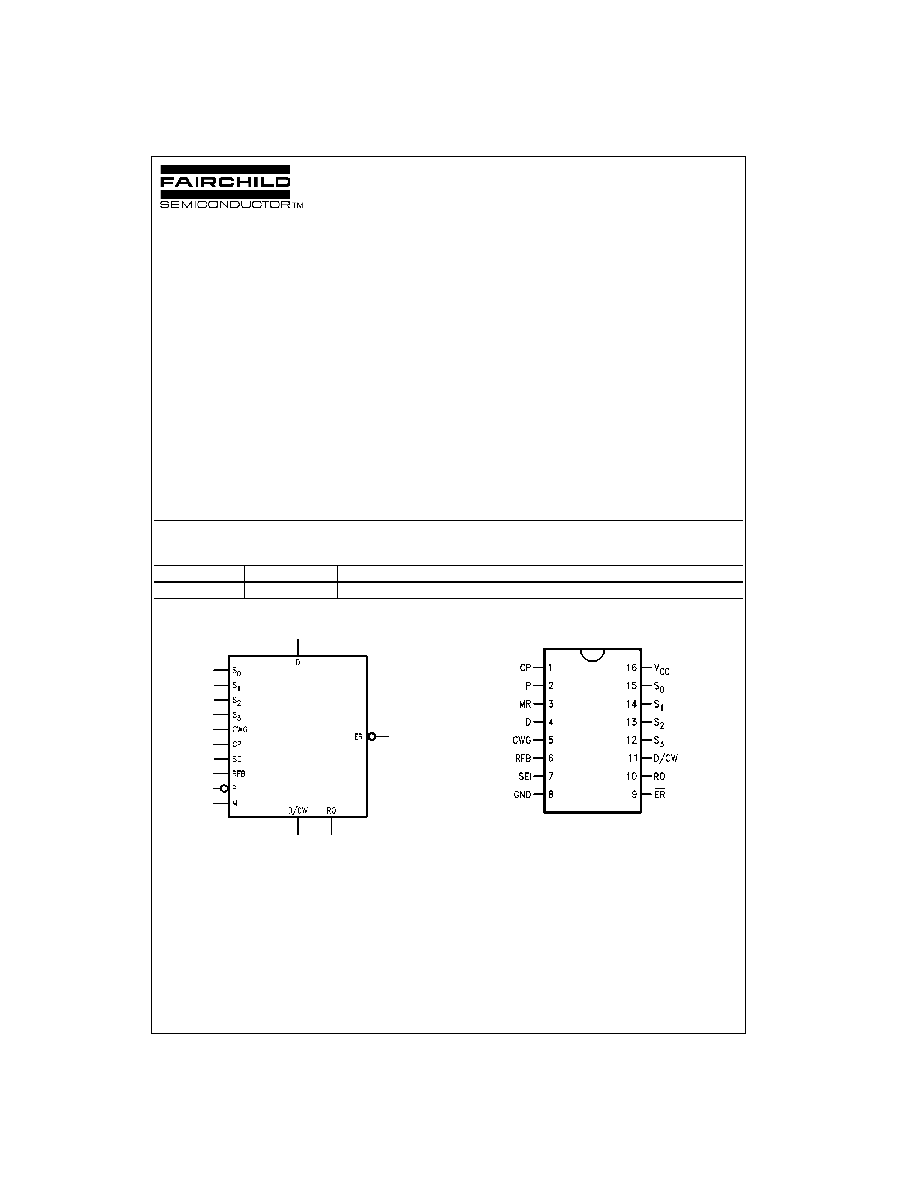
Logic Symbol
Connection Diagram
FAST
Æ
is a registered trademark of Fairchild Semiconductor Corporation.
Ethernet
Æ
is a registered trademark of Xerox Corporation.
Order Number
Package Number
Package Description
74F402PC
N16E
16-Lead Plastic Dual-In-Line Package (PDIP), JEDEC MS-001, 0.300 Wide

www.fairchildsemi.com
2
74F402
Unit Loading/Fan Out
Note 1: Open Collector
Functional Description
The 74F402 Serial Data Polynomial Generator/Checker is
an expandable 16-bit programmable device which oper-
ates on serial data streams and provides a means of
detecting transmission errors. Cyclic encoding and decod-
ing schemes for error detection are based on polynomial
manipulation in modulo arithmetic. For encoding, the data
stream (message polynomial) is divided by a selected poly-
nomial. This division results in a remainder (or residue)
which is appended to the message as check bits. For error
checking, the bit stream containing both data and check
bits is divided by the same selected polynomial. If there are
no detectable errors, this division results in a zero remain-
der. Although it is possible to choose many generating
polynomials of a given degree, standards exist that specify
a small number of useful polynomials. The 74F402 imple-
ments the polynomials listed in Table 1 by applying the
appropriate logic levels to the select pins S
0
, S
1
, S
2
and S
3
.
The 74F402 consists of a 16-bit register, a Read Only
Memory (ROM) and associated control circuitry as shown
in the Block Diagram. The polynomial control code pre-
sented at inputs S
0
, S
1
, S
2
and S
3
is decoded by the ROM,
selecting the desired polynomial or part of a polynomial by
establishing shift mode operation on the register with
Exclusive OR (XOR) gates at appropriate inputs. To gener-
ate the check bits, the data stream is entered via the Data
Inputs (D), using the LOW-to-HIGH transition of the Clock
Input (CP). This data is gated with the most significant
Register Output (RO) via the Register Feedback Input
(RFB), and controls the XOR gates. The Check Word Gen-
erate (CWG) must be held HIGH while the data is being
entered. After the last data bit is entered, the CWG is
brought LOW and the check bits are shifted out of the reg-
ister(s) and appended to the data bits (no external gating is
needed).
To check an incoming message for errors, both the data
and check bits are entered through the D Input with the
CWG Input held HIGH. The Error Output becomes valid
after the last check bit has been entered into the 'F402 by a
LOW-to-HIGH transition of CP, with the exception of the
Ethernet polynomial (see Applications paragraph). If no
detectable errors have occurred during the data transmis-
sion, the resultant internal register bits are all LOW and the
Error Output (ER) is HIGH. If a detectable error has
occurred, ER is LOW. ER remains valid until the next LOW-
to-HIGH transition of CP or until the device has been pre-
set or reset.
A HIGH on the Master Reset Input (MR) asynchronously
clears the entire register. A LOW on the Preset Input (P)
asynchronously sets the entire register with the exception
of:
1. The Ethernet residue selection, in which the registers
containing the non-zero residue are cleared;
2. The 56th order polynomial, in which the 8 least signifi-
cant register bits of the least significant device are
cleared; and,
3. Register S
=
0, in which all bits are cleared.
Pin Names
Description
U.L.
Input I
IH
/I
IL
HIGH/LOW
Output I
OH
/I
OL
S
0
≠S
3
Polynomial Select Inputs
1.0/0.67
20
µ
A/
-
0.4 mA
CWG
Check Word Generate Input
1.0/0.67
20
µ
A/
-
0.4 mA
D/CW
Serial Data/Check Word
285(100)/13.3(6.7)
-
5.7 mA(
-
2 mA)/8 mA (4 mA)
D
Data Input
1.0/0.67
20
µ
A/
-
0.4 mA
ER
Error Output
(Note 1) /26.7(13.3)
(Note 1) /16 mA (8 mA)
RO
Register Output
285(100)/13.3(6.7)
-
5.7 mA(
-
2 mA)/8 mA (4 mA)
CP
Clock Pulse
1.0/0.67
20
µ
A/
-
0.4 mA
SEI
Serial Expansion Input
1.0/0.67
20
µ
A/
-
0.4 mA
RFB
Register Feedback
1.0/0.67
20
µ
A/
-
0.4 mA
MR
Master Reset
1.0/0.67
20
µ
A/
-
0.4 mA
P
Preset
1.0/0.67
20
µ
A/
-
0.4 mA
3
www.fairchildsemi.com
7
4F402
TABLE 1.
Block Diagram
Hex
Select Code
Polynomial
Remarks
S
3
S
2
S
1
S
0
0
L
L
L
L
0
S
=
0
C
H
H
L
L
X
32
+
X
26
+
X
23
+
X
22
+
X
16
+
Ethernet
D
H
H
L
H
X
12
+
X
11
+
X
10
+
X
8
+
X
7
+
X
5
+
X
4
+
X
2
+
X
+
1
Polynomial
E
H
H
H
L
X
32
+
X
31
+
X
27
+
X
26
+
X
25
+
X
19
+
X
16
+
Ethernet
F
H
H
H
H
X
15
+
X
13
+
X
12
+
X
11
+
X
9
+
X
7
+
X
6
+
X
5
+
X
4
+
X
2
+
X
+
1
Residue
7
L
H
H
H
X
16
+
X
15
+
X
2
+
1
CRC-16
B
H
L
H
H
X
16
+
X
12
+
X
5
+
1
CRC-CCITT
3
L
L
H
H
X
56
+
X
55
+
X
49
+
X
45
+
X
41
+
2
L
L
H
L
X
39
+
X
38
+
X
37
+
X
36
+
X
31
+
56th
4
L
H
L
L
X
22
+
X
19
+
X
17
+
X
16
+
X
15
+
X
14
+
X
12
+
X
11
+
X
9
+
Order
8
H
L
L
L
X
5
+
X
+
1
5
L
H
L
H
X
48
+
X
36
+
X
35
+
9
H
L
L
H
X
23
+
X
21
+
48th
1
L
L
L
H
X
15
+
X
13
+
X
8
+
X
2
+
1
Order
6
L
H
H
L
X
32
+
X
23
+
X
21
+
32nd
A
H
L
H
L
X
11
+
X
2
+
1
Order
www.fairchildsemi.com
4
74F402
TABLE 2.
Applications
In addition to polynomial selection there are four other
capabilities provided for in the 74F402 ROM. The first is set
or clear selectability. The sixteen internal registers have the
capability to be either set or cleared when P is brought
LOW. This set or clear capability is done in four groups of 4
(see Table 2, P
0
≠P
3
). The second ROM capability (C
0
) is in
determining the polarity of the check word. As is the case
with the Ethernet polynomial the check word can be
inverted when it is appended to the data stream or as is the
case with the other polynomials, the residue is appended
with no inversion. Thirdly, the ROM contains a bit (C
1
)
which is used to select the RFB input instead of the SEI
input to be fed into the LSB. This is used when the polyno-
mial selected is actually a residue (least significant) stored
in the ROM which indicates whether the selected location
is a polynomial or a residue. If the latter, then it inhibits the
RFB input.
As mentioned previously, upon a successful data transmis-
sion, the CRC register has a zero residue. There is an
exception to this, however, with respect to the Ethernet
polynomial. This polynomial, upon a successful data trans-
mission, has a non-zero residue in the CRC register (C7 04
DD 7B)
16
. In order to provide a no-error indication, two
ROM locations have been preloaded with the residue so
that by selecting these locations and clocking the device
one additional time, after the last check bit has been
entered, will result in zeroing the CRC register. In this man-
ner a no-error indication is achieved.
With the present mix of polynomials, the largest is 56
th
order requiring four devices while the smallest is 16
th
order
requiring just one device. In order to accommodate multi-
plexing between high order polynomials (X 16
th
order) and
lower order polynomials, a location of all zeros is provided.
This allows the user to choose a lower order polynomial
even if the system is configured for a higher order one.
The 74F402 expandable CRC generator checker contains
6 popular CRC polynomials, 2-16
th
Order, 2-32
nd
Order, 1-
48
th
Order and 1-56
th
Order. The application diagram
shows the 74F402 connected for a 56
th
Order polynomial.
Also shown are the input patterns for other polynomials.
When the 74F402 is used with a gated clock, disabling the
clock in a HIGH state will ensure no erroneous clocking
occurs when the clock is re-enabled. Preset and Master
Reset are asynchronous inputs presetting the register to S
or clearing to 1s respectively (note Ethernet residue and
56
th
Order select code 8, LSB, are exceptions to this).
To generate a CRC, the pattern for the selected polynomial
is applied to the S inputs, the register is preset or cleared
as required, clock is enabled, CWG is set HIGH, data is
applied to D input, output data is on D/CW. When the last
data bit has been entered, CWG is set LOW and the regis-
ter is clocked for n bits (where n is the order of the polyno-
mial). The clock may now be stopped if desired (holding
CWG LOW and clocking the register will output zeros from
D/CW after the residue has been shifted out).
To check a CRC, the pattern for the selected polynomial is
applied to the S inputs, the register is preset or cleared as
required, clock is enabled, CWG is set HIGH, the data
stream including the CRC is applied to D input. When the
last bit of the CRC has been entered, the ER output is
checked: HIGH
=
error free data, LOW
=
corrupt data. The
clock may now be stopped if desired.
To implement polynomials of lower order than 56
th
, select
the number of packages required for the order of polyno-
mial and apply the pattern for the selected polynomial to
the S inputs (0000 on S inputs disables the package from
the feedback chain).
Select Code
P
3
P
2
P
1
P
0
C
2
C
1
C
0
Polynomial
0
0
0
0
0
1
0
0
S
=
0
C
1
1
1
1
1
0
1
Ethernet
D
1
1
1
1
1
0
1
Polynomial
E
0
0
0
0
0
0
0
Ethernet
F
0
0
0
0
0
1
0
Residue
7
1
1
1
1
1
0
0
CRC-16
B
1
1
1
1
1
0
0
CRC-CCITT
3
1
1
1
1
1
0
0
2
1
1
1
1
1
0
0
56th
4
1
1
1
1
1
0
0
Order
8
0
0
1
1
1
0
0
5
1
1
1
1
1
0
0
48th
9
1
1
1
1
1
0
0
Order
1
1
1
1
1
1
0
0
6
1
1
1
1
1
0
0
32nd
A
1
1
1
1
1
0
0
Order

5
www.fairchildsemi.com
7
4F402

www.fairchildsemi.com
6
74F402
Absolute Maximum Ratings
(Note 2)
Recommended Operating
Conditions
Note 2: Absolute maximum ratings are values beyond which the device
may be damaged or have its useful life impaired. Functional operation
under these conditions is not implied.
Note 3: Either voltage limit or current limit is sufficient to protect inputs.
DC Electrical Characteristics
Storage Temperature
-
65
∞
C to
+
150
∞
C
Ambient Temperature under Bias
-
55
∞
C to
+
125
∞
C
Junction Temperature under Bias
-
55
∞
C to
+
150
∞
C
V
CC
Pin Potential to Ground Pin
-
0.5V to
+
7.0V
Input Voltage (Note 3)
-
0.5V to
+
7.0V
Input Current (Note 3)
-
30 mA to
+
5.0 mA
Voltage Applied to Output
in HIGH State (with V
CC
=
0V)
Standard Output
-
0.5V to V
CC
3-STATE Output
-
0.5V to
+
5.5V
Current Applied to Output
in LOW State (Max)
twice the rated I
OL
(mA)
Free Air Ambient Temperature
0
∞
C to
+
70
∞
C
Supply Voltage
+
4.5V to
+
5.5V
Symbol
Parameter
Min
Typ
Max
Units
V
CC
Conditions
V
IH
Input HIGH Voltage
2.0
V
Recognized as a HIGH Signal
V
IL
Input LOW Voltage
0.8
V
Recognized as a LOW Signal
V
CD
Input Clamp Diode Voltage
-
1.2
V
Min
I
IN
=
-
18 mA
V
OH
Output HIGH
10% V
CC
2.4
V
Min
I
OH
=
-
5.7 mA (RO, D/CW)
Voltage
5% V
CC
2.7
I
OH
=
-
5.7 mA (RO, D/CW)
V
OL
Output LOW
10% V
CC
0.5
I
OL
=
16 mA (ER)
Voltage
10% V
CC
0.5
I
OL
=
8 mA (D/CW, RO)
I
IH
Input HIGH
5.0
µ
A
Max
V
IN
=
2.7V
Current
I
BVI
Input HIGH Current
7.0
µ
A
Max
V
IN
=
7.0V
Breakdown Test
I
CEX
Output HIGH
50
µ
A
Max
V
OUT
=
V
CC
Leakage Current
V
ID
Input Leakage
4.75
V
0.0
I
ID
=
1.9
µ
A
Test
All Other Pins Grounded
I
OD
Output Leakage
3.75
µ
A
0.0
V
IOD
=
150 mV
Circuit Current
All Other Pins Grounded
I
IL
Input LOW Current
-
0.4
mA
Max
V
IN
=
0.5V
I
OS
Output Short-Circuit Current
-
20
-
130
mA
Max
V
OUT
=
0V (D/CW, RO)
I
OHC
Open Collector, Output
250
µ
A
Min
V
OUT
=
V
CC
(ER)
OFF Leakage Test
I
CC
Power Supply Current
110
165
mA
Max
7
www.fairchildsemi.com
7
4F402
AC Electrical Characteristics
Symbol
Parameter
T
A
=
+
25
∞
C
T
A
=
-
55
∞
C to
+
125
∞
C
T
A
=
0
∞
C to
+
70
∞
C
Units
V
CC
=
+
5.0V
V
CC
=
+
5.0V
V
CC
=
+
5.0V
C
L
=
50 pF
C
L
=
50 pF
C
L
=
50 pF
Min
Typ
Max
Min
Max
Min
Max
f
MAX
Maximum Clock Frequency
30
45
30
30
MHz
t
PLH
Propagation Delay
8.5
15.0
19.0
7.5
26.5
7.5
21.0
ns
t
PHL
CP to D/CW
10.5
18.0
23.0
9.5
26.5
9.5
25.0
t
PLH
Propagation Delay
8.0
13.5
17.0
7.0
26.0
7.0
19.0
ns
t
PHL
CP to RO
8.0
14.0
18.0
7.0
22.5
7.0
20.0
t
PLH
Propagation Delay
15.5
26.0
33.0
14.0
38.5
14.0
35.0
ns
t
PHL
CP to ER
8.5
14.5
18.5
7.5
23.5
7.5
20.5
t
PLH
Propagation Delay
11.0
18.5
23.5
10.0
31.0
10.0
25.5
ns
t
PHL
P to D/CW
11.5
19.5
24.5
10.5
32.0
10.5
26.5
t
PLH
Propagation Delay
9.5
16.0
20.5
8.5
31.5
8.5
22.5
ns
P to RO
t
PLH
Propagation Delay
10.0
17.0
21.5
9.0
26.0
9.0
23.5
ns
P to ER
t
PLH
Propagation Delay
10.5
18.0
23.0
9.5
29.0
9.5
25.5
ns
t
PHL
MR to D/CW
11.0
19.0
24.0
10.0
28.5
10.0
26.0
t
PHL
Propagation Delay
9.0
15.5
19.5
8.0
23.5
8.0
21.5
ns
MR to RO
t
PLH
Propagation Delay
16.5
28.0
35.5
14.5
39.0
14.5
37.5
ns
MR to ER
t
PLH
Propagation Delay
6.0
10.5
13.5
5.0
19.5
5.0
15.0
ns
t
PHL
D to D/CW
7.5
12.0
16.0
6.5
20.0
6.5
18.0
t
PLH
Propagation Delay
6.5
11.0
14.0
5.5
21.5
5.5
15.5
ns
t
PHL
CWG to D/CW
7.0
12.0
15.5
6.0
21.5
6.0
17.5
t
PLH
Propagation Delay
11.5
19.5
24.5
9.0
29.0
10.5
26.5
ns
t
PHL
S
n
to D/CW
9.5
16.0
20.0
8.5
25.0
8.5
22.0

www.fairchildsemi.com
8
74F402
AC Operating Requirements
Symbol
Parameter
T
A
=
+
25
∞
C
T
A
=
-
55
∞
C to
+
125
∞
C
T
A
=
0
∞
C to
+
70
∞
C
Units
V
CC
=
+
5.0V
V
CC
=
+
5.0V
V
CC
=
+
5.0V
Min
Max
Min
Max
Min
Max
t
S
(H)
Setup Time, HIGH or LOW
4.5
6.0
5.0
ns
t
S
(L)
SEI to CP
4.5
6.0
5.0
t
H
(H)
Hold Time, HIGH or LOW
0
1.0
0
t
H
(L)
SEI to CP
0
1.0
0
t
S
(H)
Setup Time, HIGH or LOW
11.0
14.0
12.5
ns
t
S
(L)
RFB to CP
11.0
14.0
12.5
t
H
(H)
Hold Time, HIGH or LOW
0
0
0
t
H
(L)
RFB to CP
0
0
0
t
S
(H)
Setup Time, HIGH or LOW
13.5
16.0
15.0
ns
t
S
(L)
S
1
to CP
13.0
15.5
14.5
t
H
(H)
Hold Time, HIGH or LOW
0
0
0
t
H
(L)
S
1
to CP
0
0
0
t
S
(H)
Setup Time, HIGH or LOW
9.0
11.5
10.0
ns
t
S
(L)
D to CP
9.0
11.5
10.0
t
H
(H)
Hold Time, HIGH or LOW
0
0
0
t
H
(L)
D to CP
0
0
0
t
S
(H)
Setup Time, HIGH or LOW
7.0
9.0
8.0
ns
t
S
(L)
CWG to CP
5.5
8.0
6.5
t
H
(H)
Hold Time, HIGH or LOW
0
0
0
t
H
(L)
CWG to CP
0
0
0
t
W
(H)
Clock Pulse Width
4.0
7.0
4.5
ns
t
W
(L)
HIGH or LOW
4.0
5.0
4.5
t
W
(H)
MR Pulse Width, HIGH
4.0
7.0
4.5
ns
t
W
(L)
P Pulse Width, LOW
4.0
5.0
4.5
ns
t
REC
Recovery Time
3.0
4.0
3.5
ns
MR to CP
t
REC
Recovery Time
5.0
6.5
6.0
P to CP
9
www.fairchildsemi.com
7
4F402 S
e
ria
l
Data Polyno
m
i
al Generat
or/
C
hecker
Physical Dimensions
inches (millimeters) unless otherwise noted
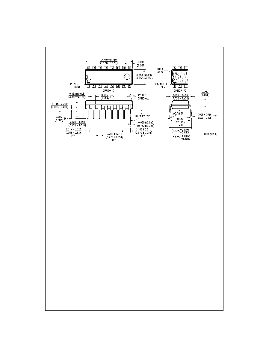
16-Lead Plastic Dual-In-Line Package (PDIP), JEDEC MS-001, 0.300 Wide
Package Number N16E
Fairchild does not assume any responsibility for use of any circuitry described, no circuit patent licenses are implied and
Fairchild reserves the right at any time without notice to change said circuitry and specifications.
LIFE SUPPORT POLICY
FAIRCHILD'S PRODUCTS ARE NOT AUTHORIZED FOR USE AS CRITICAL COMPONENTS IN LIFE SUPPORT
DEVICES OR SYSTEMS WITHOUT THE EXPRESS WRITTEN APPROVAL OF THE PRESIDENT OF FAIRCHILD
SEMICONDUCTOR CORPORATION. As used herein:
1. Life support devices or systems are devices or systems
which, (a) are intended for surgical implant into the
body, or (b) support or sustain life, and (c) whose failure
to perform when properly used in accordance with
instructions for use provided in the labeling, can be rea-
sonably expected to result in a significant injury to the
user.
2. A critical component in any component of a life support
device or system whose failure to perform can be rea-
sonably expected to cause the failure of the life support
device or system, or to affect its safety or effectiveness.
www.fairchildsemi.com