 | –≠–ª–µ–∫—Ç—Ä–æ–Ω–Ω—ã–π –∫–æ–º–ø–æ–Ω–µ–Ω—Ç: 74F403A | –°–∫–∞—á–∞—Ç—å:  PDF PDF  ZIP ZIP |
January 1989
Revised May 1999
7
4F403A
Fi
rst
-
I
n Fir
s
t-
Out (FI
F
O) Buff
er M
e
m
o
r
y
© 1999 Fairchild Semiconductor Corporation
DS009536.prf
www.fairchildsemi.com
74F403A
First-In First-Out (FIFO) Buffer Memory
General Description
The 74F403A is an expandable fall-through type high-
speed First-In First-Out (FIFO) Buffer Memory optimized
for high-speed disk or tape controllers and communication
buffer applications. It is organized as 16-words by 4-bits
and may be expanded to any number of words or any num-
ber of bits in multiples of four. Data may be entered or
extracted asynchronously in serial or parallel, allowing eco-
nomical implementation of buffer memories.
The 74F403A has 3-STATE outputs which provide added
versatility and is fully compatible with all TTL families.
Features
s
Serial or parallel input
s
Serial or parallel output
s
Expandable without external logic
s
3-STATE outputs
s
Fully compatible with all TTL families
s
Slim 24-pin package
s
9403A replacement
s
Guaranteed 4000V minimum ESD protection
Ordering Code:
Devices also available in Tape and Reel. Specify by appending the suffix letter "X" to the ordering code.
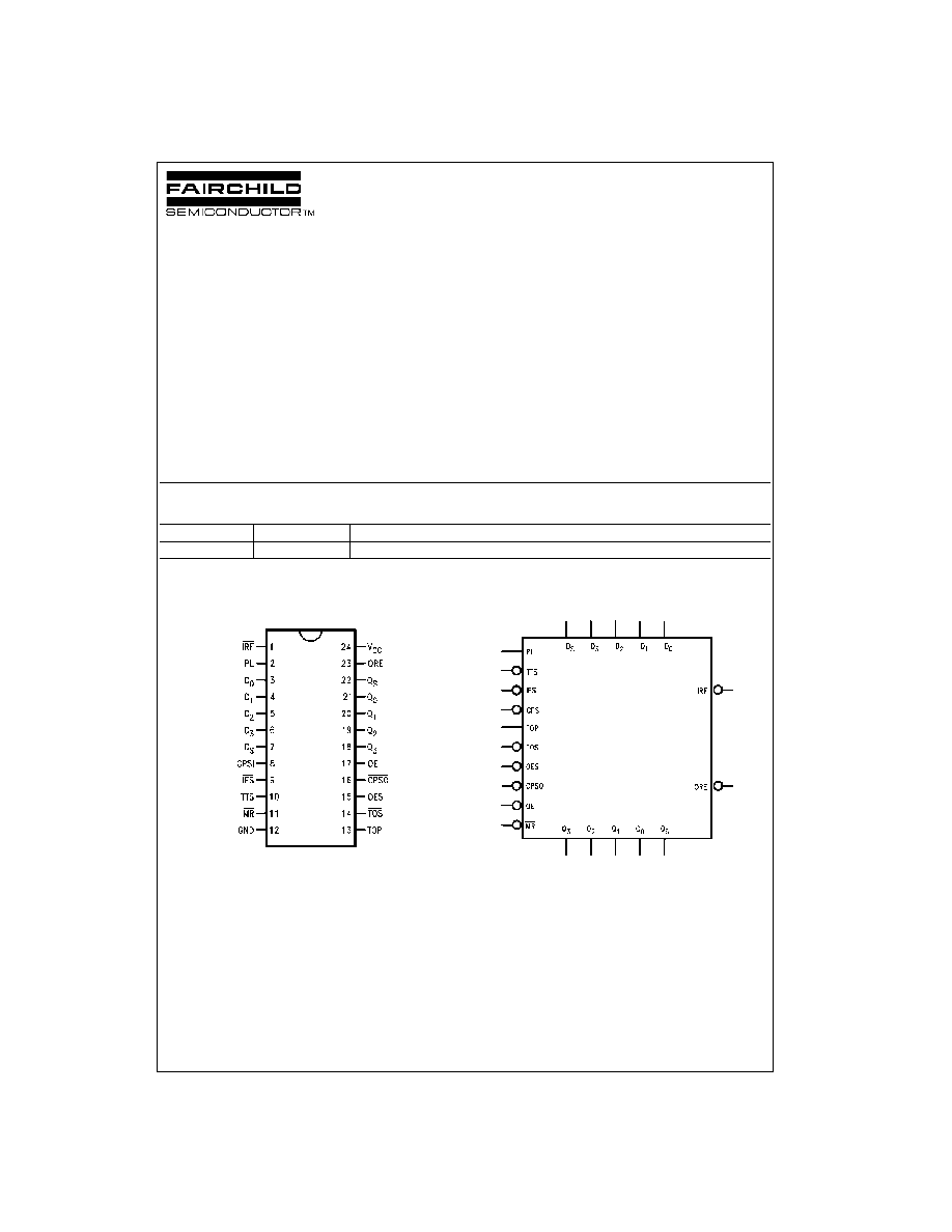
Connection Diagram
Logic Symbol
Order Number
Package Number
Package Description
74F403ASPC
N24C
24-Lead Plastic Dual-In-Line Package (PDIP), JEDEC MS-100, 0.300 Wide
www.fairchildsemi.com
2
74F40
3A
Unit Loading/Fan Out:
See Section 2 for U.L. definitions
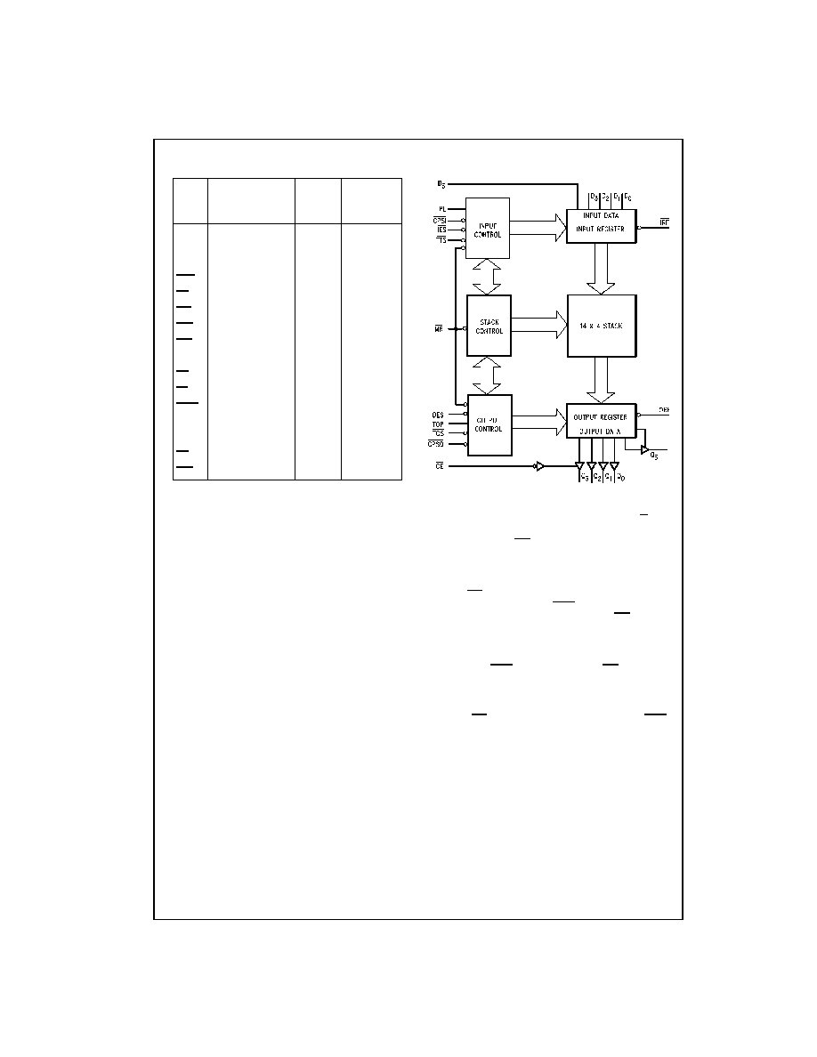
Block Diagram
Functional Description
As shown in the Block Diagram the 74F403A consists of
three sections:
1. An Input register with parallel and serial data inputs as
well as control inputs and outputs for input handshak-
ing and expansion.
2. A 4-bit wide, 14-word deep fall-through stack with self-
contained control logic.
3. An Output Register with parallel and serial data outputs
as well as control inputs and outputs for output hand-
shaking and expansion.
Since these three sections operate asynchronously and
almost independently, they will be described separately
below.
INPUT REGISTER (DATA ENTRY)
The Input Register can receive data in either bit-serial or in
4-bit parallel form. It stores this data until it is sent to the
fall-through stack and generates the necessary status and
control signals.
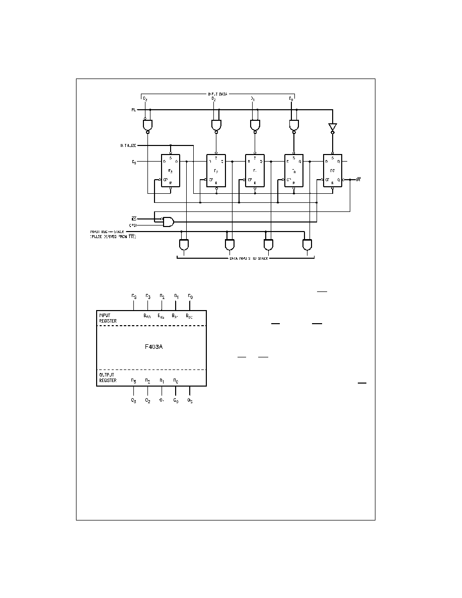
Figure 1 is a conceptual logic diagram of the input section.
As described later, this 5-bit register is initialized by setting
the F
3
flip-flop and resetting the other flip-flops. The Q out-
put of the last flip-flop (FC) is brought out as the "Input
Register Full" output (IRF). After initialization this output is
HIGH.
Parallel Entry-- A HIGH on the PL input loads the D
0
-D
3
inputs into the F
0
-F
3
flip-flops and sets the FC flip-flop. This
forces the IRF output LOW indicating that the input register
is full. During parallel entry, the CPSI input must be LOW. If
parallel expansion is not being implemented, IES must be
LOW to establish row mastership (see Expansion section).
Serial Entry-- Data on the D
S
input is serially entered into
the F
3
, F
2
, F
1
, F
0
, FC shift register on each HIGH-to-LOW
transition of the CPSI clock input, provided IES and PL are
LOW.
After the fourth clock transition, the four data bits are
located in the four flip-flops, F
0
-F
3
. The FC flip-flop is set,
forcing the IRF output LOW and internally inhibiting CPSI
clock pulses from affecting the register, Figure 2 illustrates
the final positions in a 74F403A resulting from a 64-bit
serial bit train. B
0
is the first bit, B
63
the last bit.
Pin
Description
U.L.
Input I
IH
/I
IL
Names
HIGH/LOW Output I
OH
/I
OL
D
0
-
D
3
Parallel Data Inputs
1.0/0.667
20
µ
A/400
µ
A
D
S
Serial Data Input
1.0/0.667
20
µ
A/400
µ
A
PL
Parallel Load Input
1.0/0.667
20
µ
A/400
µ
A
CPSI
Serial Input Clock
1.0/0.667
20
µ
A/400
µ
A
IES
Serial Input Enable
1.0/0.667
20
µ
A/400
µ
A
TTS
Transfer to Stack Input
1.0/0.667
20
µ
A/400
µ
A
OES
Serial Output Enable
1.0/0.667
20
µ
A/400
µ
A
TOS
Transfer Out Serial
1.0/0.667
20
µ
A/400
µ
A
TOP
Transfer Out Parallel
1.0/0.667
20
µ
A/400
µ
A
MR
Master Reset
1.0/0.667
20
µ
A/400
µ
A
OE
Output Enable
1.0/0.667
20
µ
A/400
µ
A
CPSO
Serial Output Clock
1.0/0.667
20
µ
A/400
µ
A
Q
0
-
Q
3
Parallel Data Outputs
285/26.7
5.7 mA/16 mA
Q
S
Serial Data Output
285/26.7
5.7 mA/16 mA
IRF
Input Register Full
20/13.3
-
400
µ
A/8 mA
ORE
Output Register Empty
20/13.3
-
400
µ
A/8 mA
3
www.fairchildsemi.com
7
4F403A
FIGURE 1. Conceptual Input Section
FIGURE 2. Final Positions in a 74F403A
Resulting from a 64-Bit Serial Train
Transfer to the Stack-- The outputs of Flip-Flops F
0
-F
3
feed the stack. A LOW level on the TTS input initiates a
"fall-through" action. If the top location of the stack is
empty, data is loaded into the stack and the input register is
re-initialized. Note that this initialization is postponed until
PL is LOW again. Thus, automatic FIFO action is achieved
by connecting the IRF output to the TTS input.
An RS Flip-Flop (the Request Initialization Flip-Flop shown
in Figure 10) in the control section records the fact that
data has been transferred to the stack. This prevents multi-
ple entry of the same word into the stack despite the fact
the IRF and TTS may still be LOW. The Request Initializa-
tion Flip-Flop is not cleared until PL goes LOW. Once in the
stack, data falls through the stack automatically, pausing
only when it is necessary to wait for an empty next location.
In the 74F403A as in most modern FIFO designs, the MR
input only initializes the stack control section and does not
clear the data.
OUTPUT REGISTER (DATA EXTRACTION)
The Output Register receives 4-bit data words from the
bottom stack location, stores it and outputs data on a 3-
STATE 4-bit parallel data bus or on a 3-STATE serial data
bus. The output section generates and receives the neces-
sary status and control signals. Figure 3 is a conceptual
logic diagram of the output section.

www.fairchildsemi.com
4
74F40
3A
FIGURE 3. Conceptual Output Section
Parallel Data Extraction-- When the FIFO is empty after
a LOW pulse is applied to MR, the Output Register Empty
(ORE) output is LOW. After data has been entered into the
FIFO and has fallen through to the bottom stack location, it
is transferred into the Output Register provided the "Trans-
fer Out Parallel" (TOP) input is HIGH. As a result of the
data transfer ORE goes HIGH, indicating valid data on the
data outputs (provided the 3-STATE buffer is enabled).
TOP can now be used to clock out the next word. When
TOP goes LOW, ORE will go LOW indicating that the out-
put data has been extracted, but the data itself remains on
the output bus until the next HIGH level at TOP permits the
transfer of the next word (if available) into the Output Reg-
ister. During parallel data extraction CPSO should be LOW.
TOS should be grounded for single slice operation or con-
nected to the appropriate ORE for expanded operation
(see Expansion section).
TOP is not edge triggered. Therefore, if TOP goes HIGH
before data is available from the stack, but data does
become available before TOP goes LOW again, that data
will be transferred into the Output Register. However, inter-
nal control circuitry prevents the same data from being
transferred twice. If TOP goes HIGH and returns to LOW
before data is available from the stack, ORE remains LOW
indicating that there is no valid data at the outputs.
Serial Data Extraction-- When the FIFO is empty after a
LOW pulse is applied to MR, the Output Register empty
(ORE) output is LOW. After data has been entered into the
FIFO and has fallen through to the bottom stack location, it
is transferred into the Output Register provided TOS is
LOW and TOP is HIGH. As a result of the data transfer
ORE goes HIGH indicating valid data in the register. The 3-
STATE Serial Data Output, Q
S
, is automatically enabled
and puts the first data bit on the output bus. Data is serially
shifted out on the HIGH-to-LOW transition of CPSO. To
prevent false shifting, CPSO should be LOW when the new
word is being loaded into the Output Register. The fourth
transition empties the shift register, forces ORE output
LOW and disables the serial output, Q
S
(refer to Figure 3).
For serial operation the ORE output may be tied to the TOS
input, requesting a new word from the stack as soon as the
previous one has been shifted out.

5
www.fairchildsemi.com
7
4F403A
EXPANSION
Vertical Expansion-- The 74F403A may be vertically
expanded to store more words without external parts. The
interconnection is necessary to form a 46-word by 4-bit
FIFO are shown in Figure 4. Using the same technique,
and FIFO of (15n
+
1)-words by 4-bits can be constructed,
where n is the number of devices. Note that expansion
does not sacrifice any of the 74F403A's flexibility for serial/
parallel input and output.
FIGURE 4. A Vertical Expansion Scheme
Horizontal and Vertical Expansion-- The 74F403A can
be expanded in both the horizontal and vertical directions
without any external parts and without sacrificing any of its
FIFO's flexibility for serial/parallel input and output. The
interconnections necessary to form a 31-word by 16-bit
FIFO are shown in Figure 6. Using the same technique,
any FIFO of (15m
+
1)-words by (4n)-bits can be con-
structed, where m is the number of devices in a column
and n is the number of devices in a row. Figure 7 and Fig-
ure 8 show the timing diagrams for serial data entry and
extraction for the 31-word by 16-bit FIFO shown in Figure
6. The final position of data after serial insertion of 496 bits
into the FIFO array of Figure 6 is shown in Figure 9.
Interlocking Circuitry-- Most conventional FIFO designs
provide status signals analogous to IRF and ORE. How-
ever, when these devices are operated in arrays, variations
in unit to unit operating speed require external gating to
assure all devices have completed an operation. The
74F403A incorporates simple but effective "master/slave"
interlocking circuitry to eliminate the need for external gat-
ing.
In the 74F403A array of Figure 6 devices 1 and 5 are
defined as "row masters" and the other devices are slaves
to the master in their row. No slave in a given row will initial-
ize its Input Register until it has received LOW on its IES
input from a row master or a slave of higher priority.
In a similar fashion, the ORE outputs of slaves will not go
HIGH until their OES inputs have gone HIGH.This inter-
locking scheme ensures that new input data may be
accepted by the array when the IRF output of the final
slave in that row goes HIGH and that output data for the
array may be extracted when the ORE of the final slave in
the output row goes HIGH.
The row master is established by connecting its IES input
to ground while a slave receives its IES input from the IRF
output of the next higher priority device. When an array of
74F403A FIFOs is initialized with a LOW on the MR inputs
of all devices, the IRF outputs of all devices will be HIGH.
Thus, only the row master receives a LOW on the IES input
during initialization. Figure 10 is a conceptual logic diagram
of the internal circuitry which determines master/slave
operation. Whenever MR and IES are LOW, the Master
Latch is set. Whenever TTS goes LOW the Request Initial-
ization Flip-Flop will be set. If the Master Latch is HIGH, the
Input Register will be immediately initialized and the
Request Initialization Flip-Flop reset. If the Master Latch is
reset, the Input Register is not initialized until IES goes
LOW. In array operation, activating the TTS initiates a rip-
ple input register initialization from the row master to the
last slave.
A similar operation takes place for the output register.
Either a TOS or TOP input initiates a load-from-stack oper-
ation and sets the ORE Request Flip-Flop. If the Master
Latch is set, the last Output Register Flip-Flop is set and
ORE goes HIGH. If the Master Latch is reset, the ORE out-
put will be LOW until an OES input is received.