© 1999 Fairchild Semiconductor Corporation
DS009544
www.fairchildsemi.com
April 1988
Revised August 1999
7
4F433 Fir
s
t-
In Fir
s
t-
Out (FI
F
O) Buff
er Mem
o
r
y
74F433
First-In First-Out (FIFO) Buffer Memory
General Description
The 74F433 is an expandable fall-through type high-speed
First-In First-Out (FIFO) Buffer Memory that is optimized for
high-speed disk or tape controller and communication
buffer applications. It is organized as 64-words by 4-bits
and may be expanded to any number of words or any num-
ber of bits in multiples of four. Data may be entered or
extracted asynchronously in serial or parallel, allowing eco-
nomical implementation of buffer memories.
The 74F433 has 3-STATE outputs that provide added ver-
satility, and is fully compatible with all TTL families.
Features
s
Serial or parallel input
s
Serial or parallel output
s
Expandable without additional logic
s
3-STATE outputs
s
Fully compatible with all TTL families
s
Slim 24-pin package
s
9423 replacement
Ordering Code:
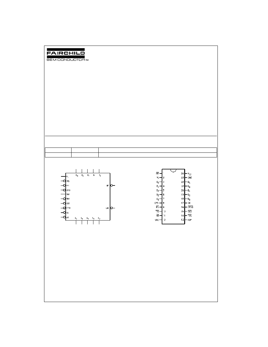
Logic Symbol
Connection Diagram
Order Number
Package Number
Package Description
74F433SPC
N24C
24-Lead Plastic Dual-In-Line Package (PDIP), JEDEC MS-100, 0.300 Wide

3
www.fairchildsemi.com
7
4F433
Functional Description
As shown in the block diagram, the 74F433 consists of
three sections:
1. An Input Register with parallel and serial data inputs,
as well as control inputs and outputs for input hand-
shaking and expansion.
2. A 4-bit-wide, 62-word-deep fall-through stack with self-
contained control logic.
3. An Output Register with parallel and serial data out-
puts, as well as control inputs and outputs for output
handshaking and expansion.
These three sections operate asynchronously and are vir-
tually independent of one another.
Input Register (Data Entry)
The Input Register can receive data in either bit-serial or 4-
bit parallel form. It stores this data until it is sent to the fall-
through stack, and also generates the necessary status
and control signals.
This 5-bit register (see Figure 1) is initialized by setting flip-
flop F
3
and resetting the other flip-flops. The Q-output of
the last flip-flop (FC) is brought out as the Input Register
Full (IRF) signal. After initialization, this output is HIGH.
Parallel Entry--A HIGH on the Parallel Load (PL) input
loads the D
0
≠D
3
inputs into the F
0
≠F
3
flip-flops and sets
the FC flip-flop. This forces the IRF output LOW, indicating
that the input register is full. During parallel entry, the Serial
Input Clock (CPSI) input must be LOW.
Serial Entry--Data on the Serial Data (D
S
) input is serially
entered into the shift register (F
3
, F
2
, F
1
, F
0
, FC) on each
HIGH-to-LOW transition of the CPSI input when the Serial
Input Enable (IES) signal is LOW. During serial entry, the
PL input should be LOW.
After the fourth clock transition, the four data bits are
located in flip-flops F
0
≠F
3
. The FC flip-flop is set, forcing
the IRF output LOW and internally inhibiting CPSI pulses
from affecting the register. Figure 2 illustrates the final posi-
tions in an 74F433 resulting from a 256-bit serial bit train
(B
0
is the first bit, B
255
the last).
FIGURE 1. Conceptual Input Section

www.fairchildsemi.com
4
74F433
FIGURE 2. Final Positions in an 74F433
Resulting from a 256-Bit Serial Train
Fall-Through Stack--The outputs of flip-flops F
0
≠F
3
feed
the stack. A LOW level on the Transfer to Stack (TTS) input
initiates a fall-through action; if the top location of the stack
is empty, data is loaded into the stack and the input register
is re-initialized. (Note that this initialization is delayed until
PL is LOW). Thus, automatic FIFO action is achieved by
connecting the IRF output to the TTS input.
An RS-type flip-flop (the initialization flip-flop) in the control
section records the fact that data has been transferred to
the stack. This prevents multiple entry of the same word
into the stack even though IRF and TTS may still be LOW;
the initialization flip-flop is not cleared until PL goes LOW.
Once in the stack, data falls through automatically, pausing
only when it is necessary to wait for an empty next location.
In the 74F433, the master reset (MR) input only initializes
the stack control section and does not clear the data.
Output Register
The Output Register (see Figure 3) receives 4-bit data
words from the bottom stack location, stores them, and out-
puts data on a 3-STATE, 4-bit parallel data bus or on a 3-
STATE serial data bus. The output section generates and
receives the necessary status and control signals.
Parallel Extraction--When the FIFO is empty after a LOW
pulse is applied to the MR input, the Output Register Empty
(ORE) output is LOW. After data has been entered into the
FIFO and has fallen through to the bottom stack location, it
is transferred into the output register, if the Transfer Out
Parallel (TOP) input is HIGH. As a result of the data trans-
fer, ORE goes HIGH, indicating valid data on the data out-
puts (provided that the 3-STATE buffer is enabled). The
TOP input can then be used to clock out the next word.
When TOP goes LOW, ORE also goes LOW, indicating
that the output data has been extracted; however, the data
itself remains on the output bus until a HIGH level on TOP
permits the transfer of the next word (if available) into the
output register. During parallel data extraction, the serial
output clock (CPSO) line should be LOW. The Transfer Out
Serial (TOS) line should be grounded for single-slice oper-
ation or connected to the appropriate ORE line for
expanded operation (refer to the "Expansion" section).
The TOP signal is not edge-triggered. Therefore, if TOP
goes HIGH before data is available from the stack but data
becomes available before TOP again goes LOW, that data
is transferred into the output register. However, internal
control circuitry prevents the same data from being trans-
ferred twice. If TOP goes HIGH and returns to LOW before
data is available from the stack, ORE remains LOW, indi-
cating that there is no valid data at the outputs.
Serial Extraction--When the FIFO is empty after a LOW
is applied to the MR input, the ORE output is LOW. After
data has been entered into the FIFO and has fallen through
to the bottom stack location, it is transferred into the output
register, if the TOS input is LOW and TOP is HIGH. As a
result of the data transfer, ORE goes HIGH, indicating that
valid data is in the register.
The 3-STATE Serial Data Output (Q
S
) is automatically
enabled and puts the first data bit on the output bus. Data
is serially shifted out on the HIGH-to-LOW transition of
CPSO. To prevent false shifting, CPSO should be LOW
when the new word is being loaded into the output register.
The fourth transition empties the shift register, forces ORE
LOW, and disables the serial output, Q
S
. For serial opera-
tion, the ORE output may be tied to the TOS input, request-
ing a new word from the stack as soon as the previous one
has been shifted out.
Expansion
Vertical Expansion--The 74F433 may be vertically
expanded, without external components, to store more
words. The interconnections necessary to form a 190-word
by 4-bit FIFO are shown in Figure 4. Using the same tech-
nique, any FIFO of (63n
+
1)-words by 4-bits can be config-
ured, where n is the number of devices. Note that
expansion does not sacrifice any of the 74F433 flexibility
for serial/parallel input and output.

