 | –≠–ª–µ–∫—Ç—Ä–æ–Ω–Ω—ã–π –∫–æ–º–ø–æ–Ω–µ–Ω—Ç: 74F521CW | –°–∫–∞—á–∞—Ç—å:  PDF PDF  ZIP ZIP |

© 2000 Fairchild Semiconductor Corporation
DS009545
www.fairchildsemi.com
April 1988
Revised October 2000
7
4
F521 8-Bi
t Ident
i
t
y
C
o
m
p
ar
ator
74F521
8-Bit Identity Comparator
General Description
The 74F521 is an expandable 8-bit comparator. It com-
pares two words of up to eight bits each and provides a
LOW output when the two words match bit for bit. The
expansion input I
A
=
B
also serves as an active LOW enable
input.
Features
s
Compares two 8-bit words in 6.5 ns typ
s
Expandable to any word length
s
20-pin package
Ordering Code:
Devices also available in Tape and Reel. Specify by appending the suffix letter "X" to the ordering code.
Logic Symbols
IEEE/IEC
Connection Diagram
Order Number
Package Number
Package Description
74F521SC
M20B
20-Lead Small Outline Integrated Circuit (SOIC), JEDEC MS-013, 0.300 Wide
74F521SJ
M20D
20-Lead Small Outline Package (SOP), EIAJ TYPE II, 5.3mm Wide
74F521MSA
MSA20
20-Lead Shrink Small Outline Package (SSOP), EIAJ TYPE II, 5.3mm Wide
74F521PC
N20A
20-Lead Plastic Dual-In-Line Package (PDIP), JEDEC MS-001, 0.300 Wide

www.fairchildsemi.com
2
74F521
Unit Loading/Fan Out
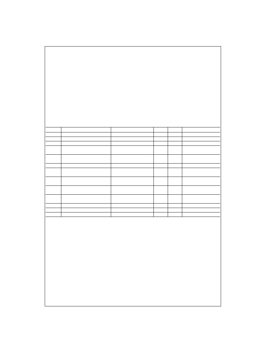
Truth Table
H
=
HIGH Voltage Level
L
=
LOW Voltage Level
Note 1: A
0
=
B
0
, A
1
=
B
1
, A
2
=
B
2
, etc.
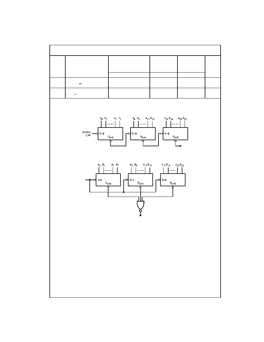
Logic Diagram
Please note that this diagram is provided only for the understanding of logic operations and should not be used to estimate propagation delays.
Pin Names
Description
U.L.
Input I
IH
/I
IL
HIGH/LOW Output I
OH
/I
OL
A
0
≠A
7
Word A Inputs
1.0/1.0
20
µ
A/
-
0.6 mA
B
0
≠B
7
Word B Inputs
1.0/1.0
20
µ
A/
-
0.6 mA
I
A
=
B
Expansion or Enable Input (Active LOW)
1.0/1.0
20
µ
A/
-
0.6 mA
O
A
=
B
Identity Output (Active LOW)
50/33.3
-
1 mA/20 mA
Inputs
Output
I
A
=
B
A, B
O
A
=
B
L
A
=
B (Note 1)
L
L
A
B
H
H
A
=
B (Note 1)
H
H
A
B
H
3
www.fairchildsemi.com
7
4
F521
Absolute Maximum Ratings
(Note 2)
Recommended Operating
Conditions
Note 2: Absolute maximum ratings are values beyond which the device
may be damaged or have its useful life impaired. Functional operation
under these conditions is not implied.
Note 3: Either voltage limit or current limit is sufficient to protect inputs.
DC Electrical Characteristics
Storage Temperature
-
65
∞
C to
+
150
∞
C
Ambient Temperature under Bias
-
55
∞
C to
+
125
∞
C
Junction Temperature under Bias
-
55
∞
C to
+
150
∞
C
V
CC
Pin Potential to Ground Pin
-
0.5V to
+
7.0V
Input Voltage (Note 3)
-
0.5V to
+
7.0V
Input Current (Note 3)
-
30 mA to
+
5.0 mA
Voltage Applied to Output
in HIGH State (with V
CC
=
0V)
Standard Output
-
0.5V to V
CC
3-STATE Output
-
0.5V to
+
5.5V
Current Applied to Output
in LOW State (Max)
twice the rated I
OL
(mA)
Free Air Ambient Temperature
0
∞
C to
+
70
∞
C
Supply Voltage
+
4.5V to
+
5.5V
Symbol
Parameter
Min
Typ
Max
Units
V
CC
Conditions
V
IH
Input HIGH Voltage
2.0
V
Recognized as a HIGH Signal
V
IL
Input LOW Voltage
0.8
V
Recognized as a LOW Signal
V
CD
Input Clamp Diode Voltage
-
1.2
V
Min
I
IN
=
-
18 mA
V
OH
Output HIGH
10% V
CC
2.5
V
Min
I
OH
=
-
1 mA
Voltage
5% V
CC
2.7
I
OH
=
-
1 mA
V
OL
Output LOW
10% V
CC
0.5
V
Min
I
OL
=
20 mA
Voltage
I
IH
Input HIGH Current
5.0
µ
A
Max
V
IN
=
2.7V
I
BVI
Input HIGH Current
7.0
µ
A
Max
V
IN
=
7.0V
Breakdown Test
I
CEX
Output HIGH
50
µ
A
Max
V
OUT
=
V
CC
Leakage Current
V
ID
Input Leakage
4.75
V
0.0
I
ID
=
1.9
µ
A
Test
All Other Pins Grounded
I
OD
Output Leakage
3.75
µ
A
0.0
V
IOD
=
150 mV
Circuit Current
All Other Pins Grounded
I
IL
Input LOW Current
-
0.6
mA
Max
V
IN
=
0.5V
I
OS
Output Short-Circuit Current
-
60
-
150
mA
Max
V
OUT
=
0V
I
CCH
Power Supply Current
21
32
mA
Max
V
O
=
HIGH
www.fairchildsemi.com
4
74F521
AC Electrical Characteristics
Applications
Ripple Expansion
Parallel Expansion
Symbol
Parameter
T
A
=
+
25
∞
C
T
A
=
-
55
∞
C to
+
125
∞
C
T
A
=
0
∞
C to
+
70
∞
C
Units
V
CC
=
+
5.0V
V
CC
=
+
5.0V
V
CC
=
+
5.0V
C
L
=
50 pF
C
L
=
50 pF
C
L
=
50 pF
Min
Typ
Max
Min
Max
Min
Max
t
PLH
Propagation Delay
3.0
7.0
10.0
3.0
14.0
3.0
11.0
ns
t
PHL
A
n
or B
n
to O
A
=
B
4.5
7.0
10.0
4.0
15.0
4.0
11.0
t
PLH
Propagation Delay
3.0
5.0
6.5
3.0
8.5
3.0
7.5
ns
t
PHL
I
A
=
B
to O
A
=
B
3.5
6.5
9.0
3.5
13.5
3.5
10.0
5
www.fairchildsemi.com
7
4
F521
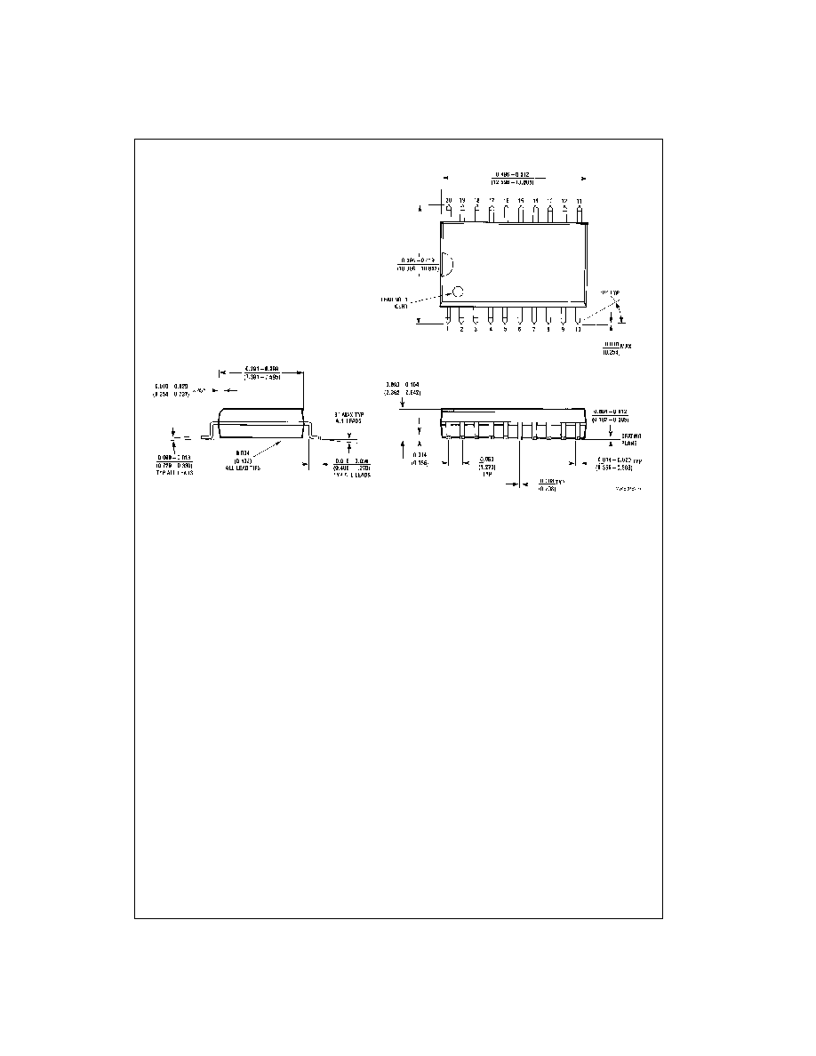
Physical Dimensions
inches (millimeters) unless otherwise noted
20-Lead Small Outline Integrated Circuit (SOIC), JEDEC MS-013, 0.300 Wide
Package Number M20B