 | –≠–ª–µ–∫—Ç—Ä–æ–Ω–Ω—ã–π –∫–æ–º–ø–æ–Ω–µ–Ω—Ç: 74F533SC | –°–∫–∞—á–∞—Ç—å:  PDF PDF  ZIP ZIP |
© 1999 Fairchild Semiconductor Corporation
DS009548
www.fairchildsemi.com
April 1988
Revised August 1999
7
4F533 O
c
t
a
l
T
r
ansparent
Latch wit
h
3-
ST
A
T
E Output
s
74F533
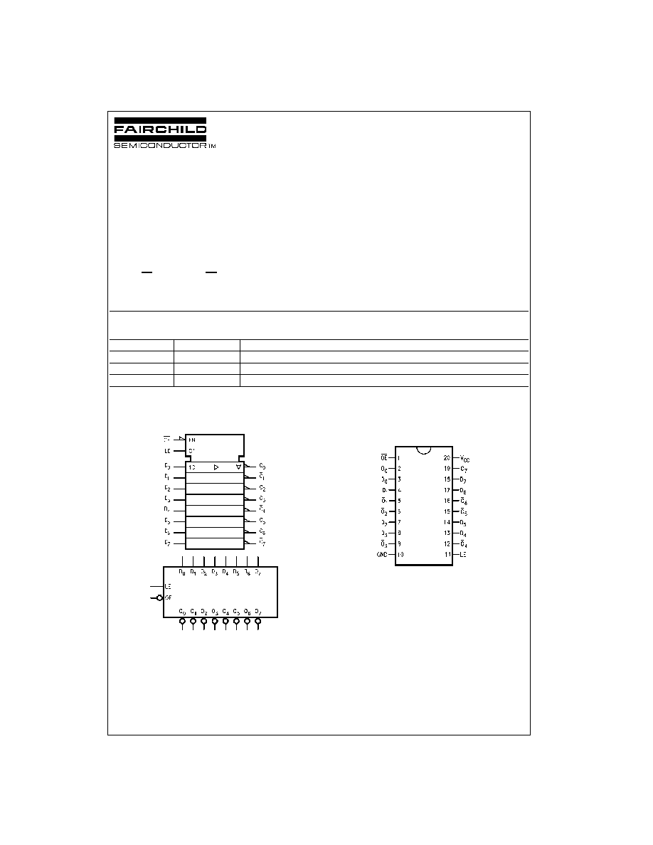
Octal Transparent Latch with 3-STATE Outputs
General Description
The 74F533 consists of eight latches with 3-STATE outputs
for bus organized system applications. The flip-flops
appear transparent to the data when Latch Enable (LE) is
HIGH. When LE is LOW, the data that meets the setup
times is latched. Data appears on the bus when the Output
Enable (OE) is LOW. When OE is HIGH the bus output is in
the high impedance state. The 74F533 is the same as the
74F373, except that the outputs are inverted.
Features
s
Eight latches in a single package
s
3-STATE outputs for bus interfacing
s
Inverted version of the 74F373
Ordering Code:
Devices also available in Tape and Reel. Specify by appending the suffix letter "X" to the ordering code.
Logic Symbols
IEEE/IEC
Connection Diagram
Order Number
Package Number
Package Description
74F533SC
M20B
20-Lead Small Outline Integrated Circuit (SOIC), JEDEC MS-013, 0.300 Wide
74F533SJ
M20D
20-Lead Small Outline Package (SOP), EIAJ TYPE II, 5.3mm Wide
74F533PC
N20A
20-Lead Plastic Dual-In-Line Package (PDIP), JEDEC MS-001, 0.300 Wide

www.fairchildsemi.com
2
74F533
Unit Loading/Fan Out
Function Table
H
=
HIGH Voltage Level
L
=
LOW Voltage Level
X
=
Immaterial
Functional Description
The 74F533 contains eight D-type latches with 3-STATE
output buffers. When the Latch Enable (LE) input is HIGH,
data on the D
n
inputs enters the latches. In this condition
the latches are transparent, i.e., a latch output will change
state each time its D input changes. When LE is LOW, the
latches store the information that was present on the D
inputs a setup time preceding the HIGH-to-LOW transition
of LE. The 3-STATE buffers are controlled by the Output
Enable (OE) input. When OE is LOW, the buffers are in the
bi-state mode. When OE is HIGH the buffers are in the high
impedance mode but this does not interfere with entering
new data into the latches.
Logic Diagram
Please note that this diagram is provided only for the understanding of logic operations and should not be used to estimate propagation delays.
Pin Names
Description
U.L.
Input I
IH
/I
IL
HIGH/LOW
Output I
OH
/I
OL
D
0
≠D
7
Data Inputs
1.0/1.0
20
µ
A/
-
0.6 mA
LE
Latch Enable Input (Active HIGH)
1.0/1.0
20
µ
A/
-
0.6 mA
OE
Output Enable Input (Active LOW)
1.0/1.0
20
µ
A/
-
0.6 mA
O
0
≠O
7
Complementary 3-STATE Outputs
150/40 (33.3)
-
3 mA/24 mA (20 mA)
Inputs
Output
LE
OE
D
O
H
L
H
L
H
L
L
H
L
L
X
O
0
X
H
X
Z

3
www.fairchildsemi.com
7
4F533
Absolute Maximum Ratings
(Note 1)
Recommended Operating
Conditions
Note 1: Absolute maximum ratings are values beyond which the device
may be damaged or have its useful life impaired. Functional operation
under these conditions is not implied.
Note 2: Either voltage limit or current limit is sufficient to protect inputs.
DC Electrical Characteristics
Storage Temperature
-
65
∞
C to
+
150
∞
C
Ambient Temperature under Bias
-
55
∞
C to
+
125
∞
C
Junction Temperature under Bias
-
55
∞
C to
+
150
∞
C
V
CC
Pin Potential to
Ground Pin
-
0.5V to
+
7.0V
Input Voltage (Note 2)
-
0.5V to
+
7.0V
Input Current (Note 2)
-
30 mA to
+
5.0 mA
Voltage Applied to Output
in HIGH State (with V
CC
=
0V)
Standard Output
-
0.5V to V
CC
3-STATE Output
-
0.5V to
+
5.5V
Current Applied to Output
in LOW State (Max)
twice the rated I
OL
(mA)
ESD Last Passing Voltage (Min)
4000V
Free Air Ambient Temperature
0
∞
C to
+
70
∞
C
Supply Voltage
+
4.5V to
+
5.5V
Symbol
Parameter
Min
Typ
Max
Units
V
CC
Conditions
V
IH
Input HIGH Voltage
2.0
V
Recognized as a HIGH Signal
V
IL
Input LOW Voltage
0.8
V
Recognized as a LOW Signal
V
CD
Input Clamp Diode Voltage
-
1.2
V
Min
I
IN
=
-
18 mA
V
OH
Output HIGH
10% V
CC
2.5
V
Min
I
OH
=
-
1 mA
Voltage
10% V
CC
2.4
I
OH
=
-
3 mA
5% V
CC
2.7
I
OH
=
-
1 mA
5% V
CC
2.7
I
OH
=
-
3 mA
V
OL
Output LOW Voltage
10% V
CC
0.5
V
Min
I
OL
=
24 mA
I
IH
Input HIGH Current
5.0
µ
A
Max
V
IN
=
2.7V
I
BVI
Input HIGH Current
7.0
µ
A
Max
V
IN
=
7.0V
Breakdown Test
I
BVIT
Input HIGH Current
0.5
mA
Max
V
IN
=
5.5V
Breakdown (I/O)
I
CEX
Output HIGH
50
µ
A
Max
V
OUT
=
V
CC
Leakage Current
V
ID
Input Leakage
4.75
V
0.0
I
ID
=
1.9
µ
A
Test
All Other Pins Grounded
I
OD
Output Leakage
3.75
µ
A
0.0
V
IOD
=
150 mV
Circuit Current
All Other Pins Grounded
I
IL
Input LOW Current
-
0.6
mA
Max
V
IN
=
0.5V
I
OZH
Output Leakage Current
50
µ
A
Max
V
OUT
=
2.7V
I
OZL
Output Leakage Current
-
50
µ
A
Max
V
OUT
=
0.5V
I
OS
Output Short-Circuit Current
-
60
-
150
mA
Max
V
OUT
=
0V
I
ZZ
Bus Drainage Test
500
µ
A
0.0V
V
OUT
=
5.25V
I
CCZ
Power Supply Current
41
61
mA
Max
V
O
=
HIGH Z

www.fairchildsemi.com
4
74F533
AC Electrical Characteristics
AC Operating Requirements
Symbol
Parameter
T
A
=
+
25
∞
C
T
A
=
-
55
∞
C to
+
125
∞
C
T
A
=
0
∞
C to
+
70
∞
C
Units
V
CC
=
+
5.0V
V
CC
=
+
5.0V
V
CC
=
+
5.0V
C
L
=
50 pF
C
L
=
50 pF
C
L
=
50 pF
Min
Typ
Max
Min
Max
Min
Max
t
PLH
Propagation Delay
4.0
6.7
9.0
4.0
12.0
4.0
10.0
ns
t
PHL
D
n
to O
n
2.5
4.4
7.0
2.5
9.0
2.5
8.0
t
PLH
Propagation Delay
5.0
7.1
11.0
5.0
14.0
5.0
13.0
ns
t
PHL
LE to O
n
3.0
4.7
7.0
3.0
9.0
3.0
8.0
t
PZH
Output Enable Time
2.0
5.9
10.0
2.0
12.5
2.0
11.0
ns
t
PZL
2.0
5.6
7.5
2.0
10.5
2.0
8.5
t
PHZ
Output Disable Time
1.5
3.4
6.5
1.5
8.5
1.5
7.0
ns
t
PLZ
1.5
2.7
5.5
1.5
7.5
1.5
6.5
Symbol
Parameter
T
A
=
+
25
∞
C
T
A
=
-
55
∞
C to
+
125
∞
C
T
A
=
0
∞
C to
+
70
∞
C
Units
V
CC
=
+
5.0V
V
CC
=
+
5.0V
V
CC
=
+
5.0V
Min
Max
Min
Max
Min
Max
t
S
(H)
Setup Time, HIGH or LOW
2.0
2.0
2.0
ns
t
S
(L)
D
n
to LE
2.0
2.0
2.0
t
H
(H)
Hold Time, HIGH or LOW
3.0
3.0
3.0
ns
t
H
(L)
D
n
to LE
3.0
3.0
3.0
t
W
(H)
LE Pulse Width, HIGH
6.0
6.0
6.0
ns
5
www.fairchildsemi.com
7
4F533
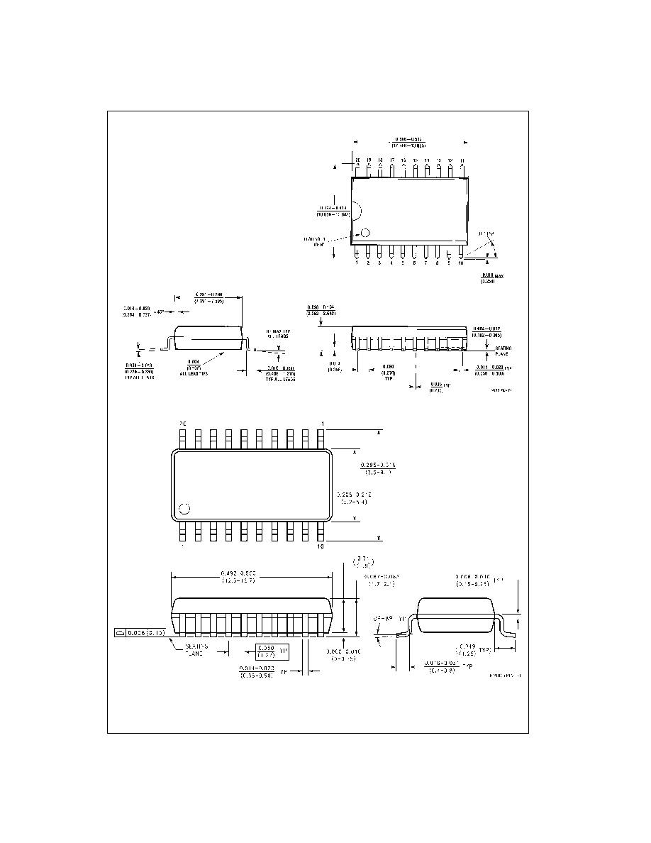
Physical Dimensions
inches (millimeters) unless otherwise noted
20-Lead Small Outline Integrated Circuit (SOIC), JEDEC MS-013, 0.300 Wide
Package Number M20B
20-Lead Small Outline Package (SOP), EIAJ TYPE II, 5.3mm Wide
Package Number M20D