 | –≠–ª–µ–∫—Ç—Ä–æ–Ω–Ω—ã–π –∫–æ–º–ø–æ–Ω–µ–Ω—Ç: 74F545PC | –°–∫–∞—á–∞—Ç—å:  PDF PDF  ZIP ZIP |
© 1999 Fairchild Semiconductor Corporation
DS009556
www.fairchildsemi.com
April 1988
Revised August 1999
7
4F545
O
c
t
a
l
Bi
dir
ecti
onal
T
r
anscei
ver
w
i
th
3-
ST
A
T
E
O
u
t
put
s
74F545
Octal Bidirectional Transceiver with 3-STATE Outputs
General Description
The 74F545 is an 8-bit, 3-STATE, high-speed transceiver. It
provides bidirectional drive for bus-oriented microproces-
sor and digital communications systems. Straight through
bidirectional transceivers are featured, with 24 mA bus
drive capability on the A Ports and 64 mA bus drive capa-
bility on the B Ports.
One input, Transmit/Receive (T/R) determines the direction
of logic signals through the bidirectional transceiver. Trans-
mit enables data from A-to-B Ports; Receive enables data
from B-to-A Ports. The Output Enable input disables both A
and B Ports by placing them in a 3-STATE condition.
Features
s
Higher drive than 8304
s
8-bit bidirectional data flow reduces system package
count
s
3-STATE inputs/outputs for interfacing with bus-oriented
systems
s
24 mA and 64 mA bus drive capability on A and B Ports,
respectively
s
Transmit/Receive and Output Enable simplify control
logic
s
Guaranteed 4000V minimum ESD protection
Ordering Code:
Devices also available in Tape and Reel. Specify by appending the suffix letter "X" to the ordering code.
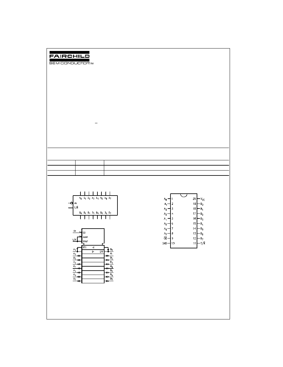
Logic Symbols
IEEE/IEC
Connection Diagram
Order Number
Package Number
Package Description
74F545SC
M20B
20-Lead Small Outline Integrated Circuit (SOIC), JEDEC MS-013, 0.300 Wide
74F545PC
N20A
20-Lead Plastic Dual-In-Line Package (PDIP), JEDEC MS-001, 0.300 Wide

www.fairchildsemi.com
2
74F545
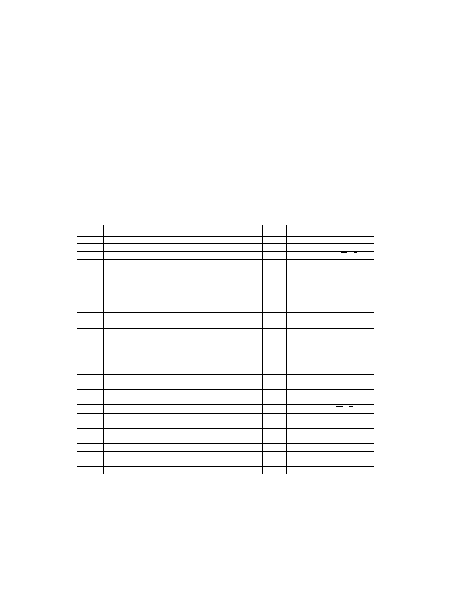
Unit Loading/Fan Out
Truth Table
H
=
HIGH Voltage Level
L
=
LOW Voltage Level
X
=
Immaterial
Z
=
High Impedance
Logic Diagram
Please note that this diagram is provided only for the understanding of logic operations and should not be used to estimate propagation delays.
Pin Names
Description
U.L.
Input I
IH
/I
IL
HIGH/LOW
Output I
OH
/I
OL
OE
Output Enable Input (Active LOW)
1.0/2.0
20
µ
A/
-
1.2 mA
T/R
Transmit/Receive Input
1.0/2.0
20
µ
A/
-
1.2 mA
A
0
≠A
7
Side A 3-STATE Inputs or
3.5/1.083
70
µ
A/
-
650
µ
A
3-STATE Outputs
150/40 (33.3)
-
3 mA/24 mA (20 mA)
B
0
≠B
7
Side B 3-STATE Inputs or
3.5/1.083
70
µ
A/
-
650
µ
A
3-STATE Outputs
600/106.6 (80)
-
12 mA/64 mA (48 mA)
Inputs
Outputs
OE
T/R
L
L
Bus B Data to Bus A
L
H
Bus A Data to Bus B
H
X
High Z
3
www.fairchildsemi.com
7
4F545
Absolute Maximum Ratings
(Note 1)
Recommended Operating
Conditions
Note 1: Absolute maximum ratings are values beyond which the device
may be damaged or have its useful life impaired. Functional operation
under these conditions is not implied.
Note 2: Either voltage limit or current limit is sufficient to protect inputs.
DC Electrical Characteristics
Storage Temperature
-
65
∞
C to
+
150
∞
C
Ambient Temperature under Bias
-
55
∞
C to
+
125
∞
C
Junction Temperature under Bias
-
55
∞
C to
+
150C
V
CC
Pin Potential to Ground Pin
-
0.5V to
+
7.0V
Input Voltage (Note 2)
-
0.5V to
+
7.0V
Input Current (Note 2)
-
30 mA to
+
5.0 mA
Voltage Applied to Output
in HIGH State (with V
CC
=
0V)
Standard Output
-
0.5V to V
CC
3-STATE Output
-
0.5V to
+
5.5V
Current Applied to Output
in LOW State (Max)
twice the rated I
OL
(mA)
ESD Last Passing Voltage (Min)
4000V
Free Air Ambient Temperature
0
∞
C to
+
70
∞
C
Supply Voltage
+
4.5V to
+
5.5V
Symbol
Parameter
Min
Typ
Max
Units
V
CC
Conditions
V
IH
Input HIGH Voltage
2.0
V
Recognized as a HIGH Signal
V
IL
Input LOW Voltage
0.8
V
Recognized as a LOW Signal
V
CD
Input Clamp Diode Voltage
-
1.2
V
Min
I
IN
=
-
18 mA (OE, T/R)
V
OH
Output HIGH
10% V
CC
2.5
V
Min
I
OH
=
-
1 mA (A
n
)
Voltage
10% V
CC
2.4
I
OH
=
-
3 mA (A
n
)
10% V
CC
2.0
I
OH
=
-
15 mA (B
n
)
5% V
CC
2.7
I
OH
=
-
1 mA (A
n
)
5% V
CC
2.7
I
OH
=
-
3 mA (A
n
)
V
OL
Output LOW
10% V
CC
0.5
V
Min
I
OL
=
24 mA (A
n
)
Voltage
10% V
CC
0.55
I
OL
=
64 mA (B
n
)
I
IH
Input HIGH
5.0
µ
A
Max
V
IN
=
2.7V (OE, T/R)
Current
I
BVI
Input HIGH Current
7.0
µ
A
Max
V
IN
=
7.0V (OE, T/R)
Breakdown Test
I
BVIT
Input HIGH Current
0.5
mA
Max
V
IN
=
5.5V (A
n
, B
n
)
Breakdown (I/O)
I
CEX
Output HIGH
50
µ
A
Max
V
OUT
=
V
CC
Leakage Current
V
ID
Input Leakage
4.75
V
0.0
I
ID
=
1.9
µ
A
Test
All Other Pins Grounded
I
OD
Output Leakage
3.75
µ
A
0.0
V
IOD
=
150 mV
Circuit Current
All Other Pins Grounded
I
IL
Input LOW Current
-
1.2
mA
Max
V
IN
=
0.5V (OE, T/R)
I
IH
+
I
OZH
Output Leakage Current
70
µ
A
Max
V
OUT
=
2.7V (A
n
, B
n
)
I
IL
+
I
OZL
Output Leakage Current
-
650
µ
A
Max
V
OUT
=
0.5V (A
n
, B
n
)
I
OS
Output Short-Circuit Current
-
60
-
150
mA
Max
V
OUT
=
0V (A
n
)
-
100
-
225
V
OUT
=
0V (B
n
)
I
ZZ
Bus Drainage Test
500
µ
A
0.0V
V
OUT
=
5.25V
I
CCH
Power Supply Current
70
90
mA
Max
V
O
=
HIGH
I
CCL
Power Supply Current
95
120
mA
Max
V
O
=
LOW
I
CCZ
Power Supply Current
85
110
mA
Max
V
O
=
HIGH Z
www.fairchildsemi.com
4
74F545
AC Electrical Characteristics
Symbol
Parameter
T
A
=
+
25
∞
C
T
A
=
-
55
∞
C to
+
125
∞
C
T
A
=
0
∞
C to
+
70
∞
C
Units
V
CC
=
+
5.0V
V
CC
=
+
5.0V
V
CC
=
+
5.0V
C
L
=
50 pF
C
L
=
50 pF
C
L
=
50 pF
Min
Typ
Max
Min
Max
Min
Max
t
PLH
Propagation Delay
2.5
4.2
6.0
2.0
7.5
2.5
7.0
ns
t
PHL
A
n
to B
n
or B
n
to A
n
2.5
4.6
6.0
2.0
7.5
2.5
7.0
t
PZH
Output Enable Time
3.0
5.3
7.0
2.5
9.0
3.0
8.0
ns
t
PZL
3.5
6.0
8.0
3.0
10.0
3.5
9.0
t
PHZ
Output Disable Time
3.0
5.0
6.5
2.5
9.0
3.0
7.5
t
PLZ
2.0
5.0
6.5
2.0
10.0
2.0
7.5
5
www.fairchildsemi.com
7
4F545
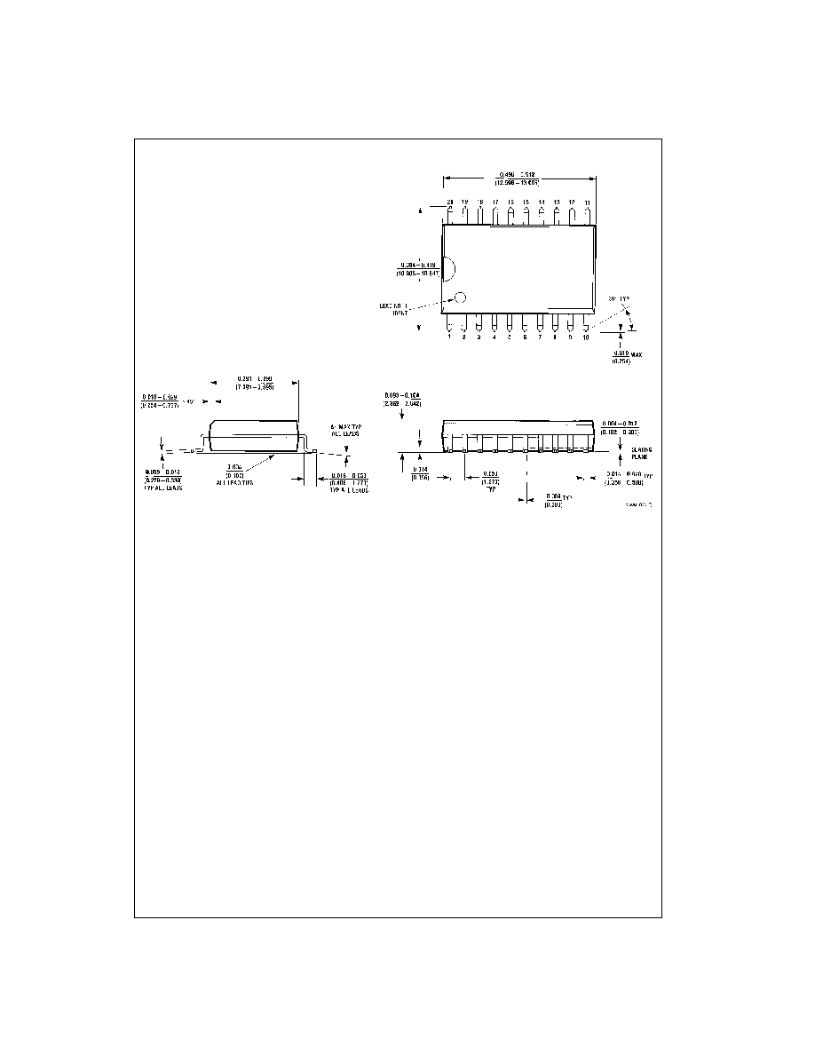
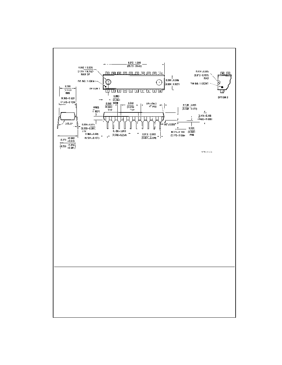
Physical Dimensions
inches (millimeters) unless otherwise noted
20-Lead Small Outline Integrated Circuit (SOIC), JEDEC MS-013, 0.300 Wide
Package Number M20B
www.fairchildsemi.com
6
74F
545
Oct
a
l Bidi
rec
t
i
onal T
r
an
sceive
r
wi
th 3-
S
T
A
T
E O
u
t
puts
Physical Dimensions
inches (millimeters) unless otherwise noted (Continued)
20-Lead Plastic Dual-In-Line Package (PDIP), JEDEC MS-001, 0.300 Wide
Package Number N20A
Fairchild does not assume any responsibility for use of any circuitry described, no circuit patent licenses are implied and
Fairchild reserves the right at any time without notice to change said circuitry and specifications.
LIFE SUPPORT POLICY
FAIRCHILD'S PRODUCTS ARE NOT AUTHORIZED FOR USE AS CRITICAL COMPONENTS IN LIFE SUPPORT
DEVICES OR SYSTEMS WITHOUT THE EXPRESS WRITTEN APPROVAL OF THE PRESIDENT OF FAIRCHILD
SEMICONDUCTOR CORPORATION. As used herein:
1. Life support devices or systems are devices or systems
which, (a) are intended for surgical implant into the
body, or (b) support or sustain life, and (c) whose failure
to perform when properly used in accordance with
instructions for use provided in the labeling, can be rea-
sonably expected to result in a significant injury to the
user.
2. A critical component in any component of a life support
device or system whose failure to perform can be rea-
sonably expected to cause the failure of the life support
device or system, or to affect its safety or effectiveness.
www.fairchildsemi.com