 | –≠–ª–µ–∫—Ç—Ä–æ–Ω–Ω—ã–π –∫–æ–º–ø–æ–Ω–µ–Ω—Ç: 74F651SPC | –°–∫–∞—á–∞—Ç—å:  PDF PDF  ZIP ZIP |
© 1999 Fairchild Semiconductor Corporation
DS009581
www.fairchildsemi.com
March 1988
Revised August 1999
7
4F651
∑
74F652
T
r
anscei
vers/
Regist
ers
74F651 ∑ 74F652
Transceivers/Registers
General Description
These devices consist of bus transceiver circuits with D-
type flip-flops, and control circuitry arranged for multiplexed
transmission of data directly from the input bus or from
internal registers. Data on the A or B bus will be clocked
into the registers as the appropriate clock pin goes to HIGH
logic level. Output Enable pins (OEAB, OEBA) are pro-
vided to control the transceiver function.
Features
s
Independent registers for A and B buses
s
Multiplexed real-time and stored data
s
Choice of non-inverting and inverting data paths
74F651 inverting
74F652 non-inverting
Ordering Code:
Devices also available in Tape and Reel. Specify by appending the suffix letter "X" to the ordering code.
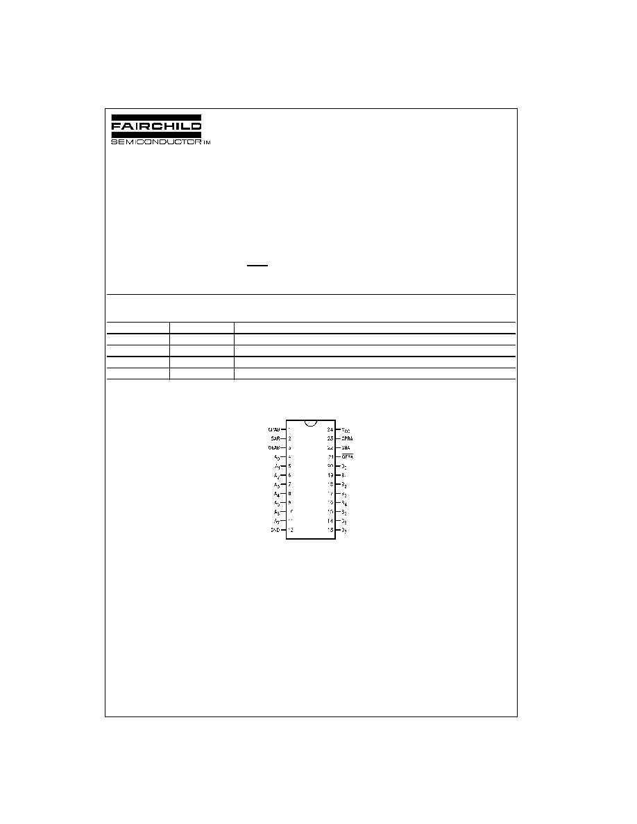
Connection Diagram
Order Number
Package Number
Package Description
74F651SC
M24B
24-Lead Small Outline Integrated Circuit (SOIC), JEDEC MS-013, 0.300 Wide
74F651SPC
N24C
24-Lead Plastic Dual-In-Line Package (PDIP), JEDEC MS-100, 0.300 Wide
74F652SC
M24B
24-Lead Small Outline Integrated Circuit (SOIC), JEDEC MS-013, 0.300 Wide
74F652SPC
N24C
24-Lead Plastic Dual-In-Line Package (PDIP), JEDEC MS-100, 0.300 Wide

www.fairchildsemi.com
2
7
4F651
∑
74F652
Logic Symbols
74F651
IEEE/IEC
74F651
74F652
IEEE/IEC
74F652
Unit Loading/Fan Out
Function Table
H
=
HIGH Voltage Level
X
=
Immaterial
L
=
LOW Voltage Level
=
LOW-to-HIGH Clock Transition
Note 1: The data output functions may be enabled or disabled by various signals at OEAB or OEBA inputs. Data input functions are always enabled,
i.e., data at the bus pins will be stored on every LOW-to-HIGH transition on the clock inputs.
Pin Names
Description
U.L.
Input I
IH
/I
IL
HIGH/LOW
Output I
OH
/I
OL
A
0
≠A
7
, B
0
≠B
7
A and B Inputs/
1.0/1.0
20
µ
A/
-
0.6 mA
3-STATE Outputs
600/106.6 (80)
-
12 mA/64 mA (48 mA)
CPAB, CPBA
Clock Inputs
1.0/1.0
20
µ
A/
-
0.6 mA
SAB, SBA
Select Inputs
1.0/1.0
20
µ
A/
-
0.6 mA
OEAB, OEBA
Output Enable Inputs
1.0/1.0
20
µ
A/
-
0.6 mA
Inputs
Inputs/Outputs (Note 1)
Operating Mode
OEAB OEBA CPAB CPBA SAB SBA
A
0
thru A
7
B
0
thru B
7
L
H
H or L H or L
X
X
Input
Input
Isolation
L
H
X
X
Store A and B Data
X
H
H or L
X
X
Input
Not Specified Store A, Hold B
H
H
X
X
Input
Output
Store A in Both Registers
L
X
H or L
X
X
Not Specified Input
Hold A, Store B
L
L
X
X
Output
Input
Store B in Both Registers
L
L
X
X
X
L
Output
Input
Real-Time B Data to A Bus
L
L
X
H or L
X
H
Store B Data to A Bus
H
H
X
X
L
X
Input
Output
Real-Time A Data to B Bus
H
H
H or L
X
H
X
Stored A Data to B Bus
H
L
H or L H or L
H
H
Output
Output
Stored A Data to B Bus and
Stored B Data to A Bus
3
www.fairchildsemi.com
7
4F651
∑
74F652
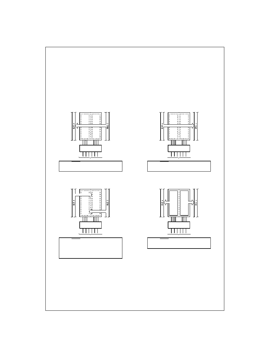
Functional Description
In the transceiver mode, data present at the HIGH imped-
ance port may be stored in either the A or B register or
both.
The select (SAB, SBA) controls can multiplex stored and
real-time.
The examples in Figure 1 demonstrate the four fundamen-
tal bus-management functions that can be performed with
the Octal bus transceivers and receivers.
Data on the A or B data bus, or both can be stored in the
internal D flip-flop by LOW-to-HIGH transitions at the
appropriate Clock Inputs (CPAB, CPBA) regardless of the
Select or Output Enable Inputs. When SAB and SBA are in
the real time transfer mode, it is also possible to store data
without using the internal D flip-flops by simultaneously
enabling OEAB and OEBA. In this configuration each Out-
put reinforces its Input. Thus when all other data sources to
the two sets of bus lines are in a HIGH impedance state,
each set of bus lines will remain at its last state.
Note A: Real-Time
Transfer Bus B to Bus A
Note B: Real-Time
Transfer Bus A to Bus B
Note C: Storage
Note D: Transfer Storage
Data to A or B
FIGURE 1.
OEAB OEBA CPAB CPBA SAB SBA
L
L
X
X
X
L
OEAB OEBA CPAB CPBA SAB SBA
H
H
X
X
L
X
OEAB OEBA CPAB CPBA SAB SBA
X
H
X
X
X
L
X
X
X
X
L
H
X
X
OEAB OEBA CPAB CPBA SAB SBA
H
L
H or L H or L
H
X
www.fairchildsemi.com
4
7
4F651
∑
74F652
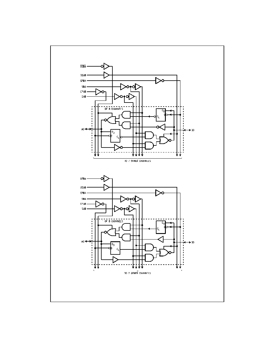
Logic Diagrams
74F652
Please note that this diagram is provided only for the understanding of logic operations and should not be used to estimate propagation delays.
74F651
Please note that this diagram is provided only for the understanding of logic operations and should not be used to estimate propagation delays.
5
www.fairchildsemi.com
7
4F651
∑
74F652
Absolute Maximum Ratings
(Note 2)
Recommended Operating
Conditions
Note 2: Absolute maximum ratings are values beyond which the device
may be damaged or have its useful life impaired. Functional operation
under these conditions is not implied.
Note 3: Either voltage limit or current limit is sufficient to protect inputs.
DC Electrical Characteristics
Storage Temperature
-
65
∞
C to
+
150
∞
C
Ambient Temperature under Bias
-
55
∞
C to
+
125
∞
C
Junction Temperature under Bias
-
55
∞
C to
+
150
∞
C
V
CC
Pin Potential to Ground Pin
-
0.5V to
+
7.0V
Input Voltage (Note 3)
-
0.5V to
+
7.0V
Input Current (Note 3)
-
30 mA to
+
5.0 mA
Voltage Applied to Output
in HIGH State (with V
CC
=
0V)
Standard Output
-
0.5V to V
CC
3-STATE Output
-
0.5V to
+
5.5V
Current Applied to Output
in LOW State (Max)
twice the rated I
OL
(mA)
ESD Last Passing Voltage (Min)
4000V
Free Air Ambient Temperature
0
∞
C to
+
70
∞
C
Supply Voltage
+
4.5V to
+
5.5V
Symbol
Parameter
Min
Typ
Max
Units
V
CC
Conditions
V
IH
Input HIGH Voltage
2.0
V
Recognized as a HIGH Signal
V
IL
Input LOW Voltage
0.8
V
Recognized as a LOW Signal
V
CD
Input Clamp Diode Voltage
-
1.2
V
Min
I
IN
=
-
18 mA (Non I/O Pins)
V
OH
Output HIGH
10% V
CC
2.0
V
Min
I
OH
=
-
15 mA (A
n
, B
n
)
Voltage
V
OL
Output LOW
10% V
CC
0.55
V
Min
I
OL
=
64 mA (A
n
, B
n
)
Voltage
I
IH
Input HIGH
5.0
µ
A
Max
V
IN
=
2.7V
Current
(Non I/O Pins)
I
BVI
Input HIGH Current
7.0
µ
A
Max
V
IN
=
7.0V
Breakdown Test
I
BVIT
Input HIGH Current
0.5
mA
Max
V
IN
=
5.5V
Breakdown (I/O)
(A
n
, B
n
)
I
CEX
Output HIGH
50
µ
A
Max
V
OUT
=
V
CC
Leakage Current
V
ID
Input Leakage
4.75
V
0.0
I
ID
=
1.9
µ
A
Test
All Other Pins Grounded
I
OD
Output Leakage
3.75
µ
A
0.0
VI
IOD
=
150 mV
Circuit Current
All Other Pins Grounded
I
IL
Input LOW Current
-
0.6
mA
Max
V
IN
=
0.5V (Non I/O Pins)
I
IH
+
I
OZH
Output Leakage Current
70
µ
A
Max
V
OUT
=
2.7V (A
n
, B
n
)
I
IL
+
I
OZL
Output Leakage Current
-
650
µ
A
Max
V
OUT
=
0.5V (A
n
, B
n
)
I
OS
Output Short-Circuit Current
-
100
-
225
mA
Max
V
OUT
=
0V
I
ZZ
Bus Drainage Test
500
µ
A
0.0V
V
OUT
=
5.25V
I
CCH
Power Supply Current
105
135
mA
Max
V
O
=
HIGH
I
CCL
Power Supply Current
118
150
mA
Max
V
O
=
LOW
I
CCZ
Power Supply Current
115
150
mA
Max
V
O
=
HIGH Z
www.fairchildsemi.com
6
7
4F651
∑
74F652
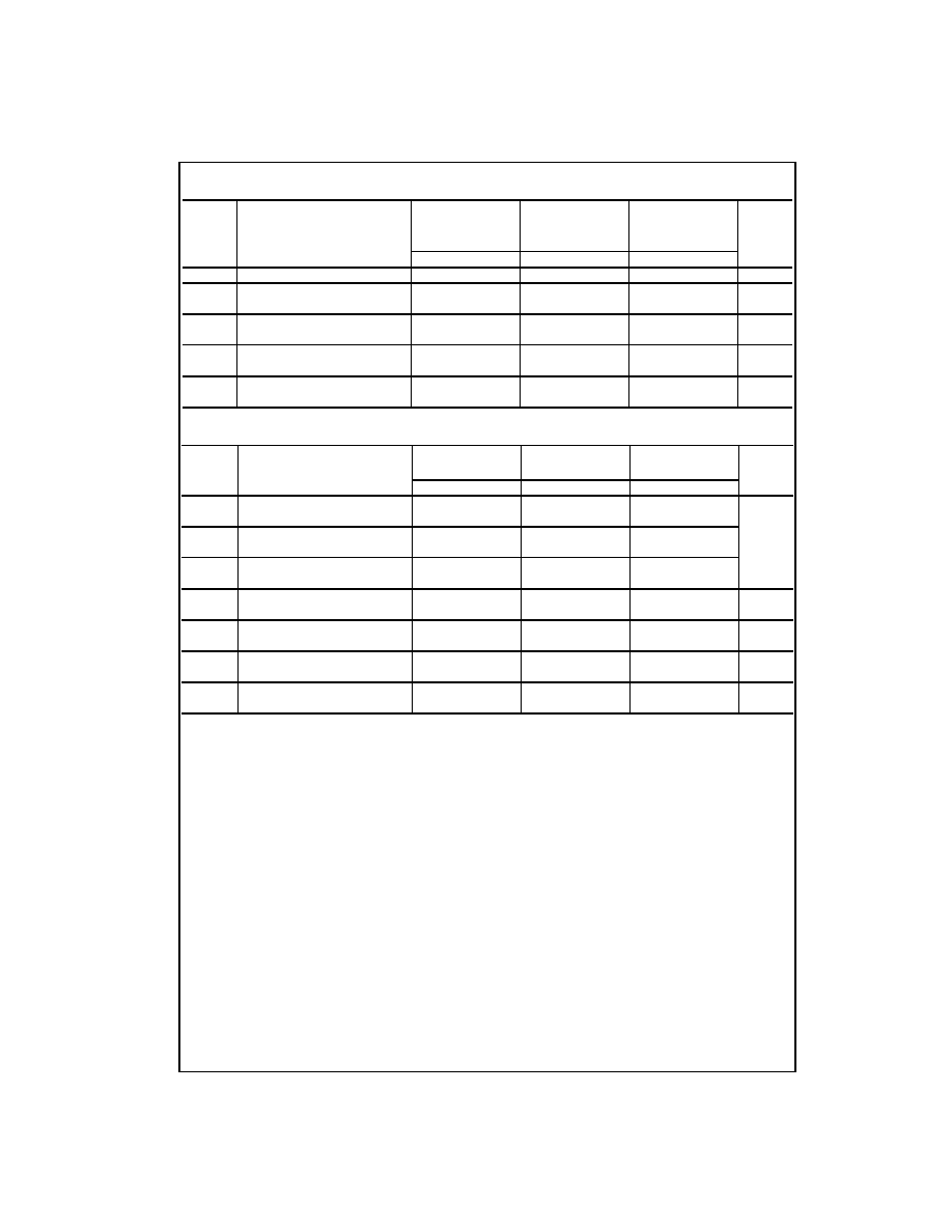
AC Electrical Characteristics
AC Operating Requirements
Symbol
Parameter
T
A
=
+
25
∞
C
T
A
=
-
55
∞
C to
+
125
∞
C
T
A
=
0
∞
C to
+
70
∞
C
Units
V
CC
=
+
5.0V
V
CC
=
+
5.0V
V
CC
=
+
5.0V
C
L
=
50 pF
C
L
=
50 pF
C
L
=
50 pF
Min
Max
Min
Max
Min
Max
f
MAX
Max. Clock Frequency
90
75
90
MHz
t
PLH
Propagation Delay
2.0
7.0
2.0
8.5
2.0
8.0
ns
t
PHL
Clock to Bus
2.0
8.0
2.0
9.5
2.0
9.0
t
PLH
Propagation Delay
2.0
8.5
1.0
9.0
2.0
9.0
ns
t
PHL
Bus to Bus (74F651)
1.0
7.5
1.0
8.0
1.0
8.0
t
PLH
Propagation Delay
1.0
7.0
1.0
8.0
1.0
7.5
ns
t
PHL
Bus to Bus (74F652)
1.0
6.5
1.0
8.0
1.0
7.0
t
PLH
Propagation Delay
2.0
8.5
2.0
11.0
2.0
9.5
ns
t
PHL
SBA or SAB to A or B
2.0
8.0
2.0
10.0
2.0
9.0
Symbol
Parameter
T
A
=
+
25
∞
C
T
A
=
-
55
∞
C to
+
125
∞
C
T
A
=
0
∞
C to
+
70
∞
C
Units
V
CC
=
+
5.0V
V
CC
=
+
5.0V
V
CC
=
+
5.0V
Min
Max
Min
Max
Min
Max
t
PZH
Enable Time
2.0
9.5
2.0
10.0
2.0
10.0
ns
t
PZL
*OEBA to A
2.0
12.0
2.0
10.0
2.0
12.5
t
PHZ
Disable Time
1.0
7.5
1.0
9.0
1.0
8.0
t
PLZ
*OEBA to A
2.0
8.5
1.0
9.0
2.0
9.0
t
PZH
Enable Time
2.0
9.5
2.0
10.0
2.0
10.0
t
PZL
OEAB to B
3.0
13.0
2.0
12.0
3.0
14.0
t
PHZ
Disable Time
2.0
9.0
1.0
9.0
2.0
10.0
ns
t
PLZ
OEAB to B
2.0
10.5
1.0
12.0
2.0
11.0
t
S
(H)
Setup Time, HIGH or
5.0
5.0
5.0
ns
t
S
(L)
LOW, Bus to Clock
5.0
5.0
5.0
t
H
(H)
Hold Time, HIGH or
2.0
2.5
2.0
ns
t
H
(L)
LOW, Bus to Clock
2.0
2.5
2.0
t
W
(H)
Clock Pulse Width
5.0
5.0
5.0
ns
t
W
(L)
HIGH or LOW
5.0
5.0
5.0

7
www.fairchildsemi.com
7
4F651
∑
74F652
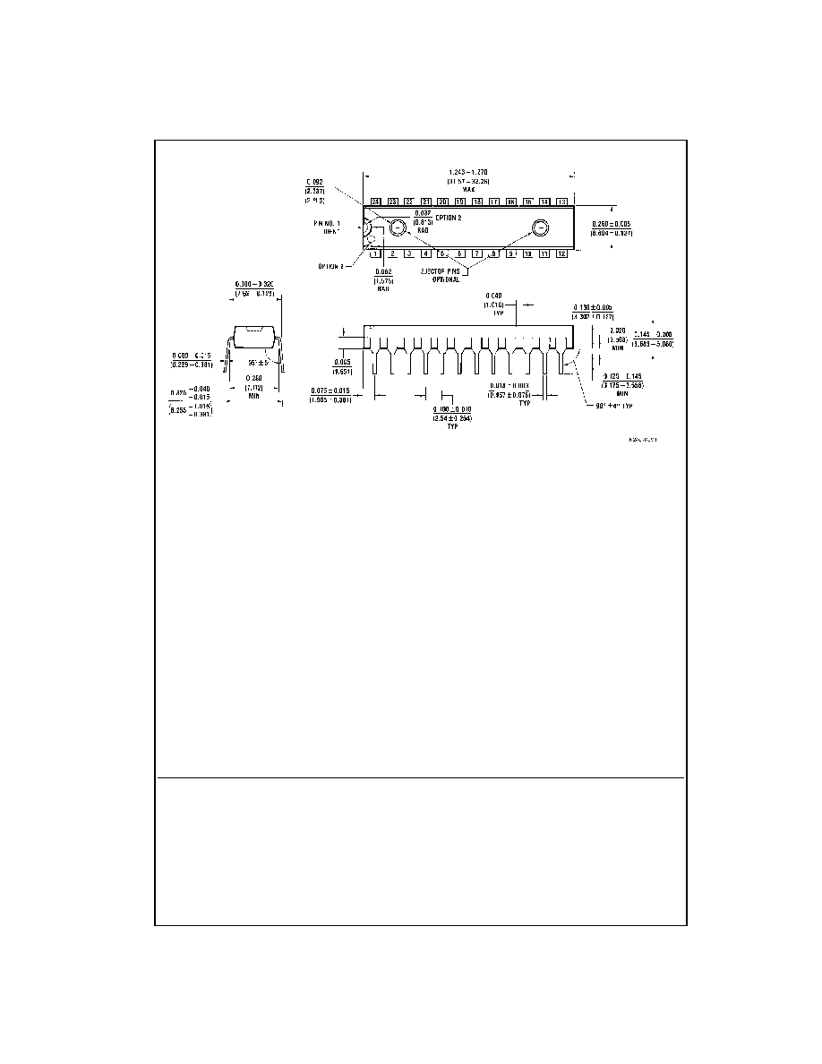
Physical Dimensions
inches (millimeters) unless otherwise noted
24-Lead Small Outline Integrated Circuit (SOIC), JEDEC MS-013, 0.300 Wide
Package Number M24B
www.fairchildsemi.com
8
7
4F651
∑
74F652
T
r
anscei
vers/
Regist
ers
Physical Dimensions
inches (millimeters) unless otherwise noted (Continued)
24-Lead Plastic Dual-In-Line Package (PDIP), JEDEC MS-100, 0.300 Wide
Package Number N24C
Fairchild does not assume any responsibility for use of any circuitry described, no circuit patent licenses are implied and
Fairchild reserves the right at any time without notice to change said circuitry and specifications.
LIFE SUPPORT POLICY
FAIRCHILD'S PRODUCTS ARE NOT AUTHORIZED FOR USE AS CRITICAL COMPONENTS IN LIFE SUPPORT
DEVICES OR SYSTEMS WITHOUT THE EXPRESS WRITTEN APPROVAL OF THE PRESIDENT OF FAIRCHILD
SEMICONDUCTOR CORPORATION. As used herein:
1. Life support devices or systems are devices or systems
which, (a) are intended for surgical implant into the
body, or (b) support or sustain life, and (c) whose failure
to perform when properly used in accordance with
instructions for use provided in the labeling, can be rea-
sonably expected to result in a significant injury to the
user.
2. A critical component in any component of a life support
device or system whose failure to perform can be rea-
sonably expected to cause the failure of the life support
device or system, or to affect its safety or effectiveness.
www.fairchildsemi.com