 | –≠–ª–µ–∫—Ç—Ä–æ–Ω–Ω—ã–π –∫–æ–º–ø–æ–Ω–µ–Ω—Ç: 74F676 | –°–∫–∞—á–∞—Ç—å:  PDF PDF  ZIP ZIP |
© 1999 Fairchild Semiconductor Corporation
DS009588
www.fairchildsemi.com
April 1988
Revised August 1999
7
4F676
16-Bi
t
Seri
al/
P
aral
le
l-
In,
Ser
i
al
-Out
Shi
f
t
Regi
st
er
74F676
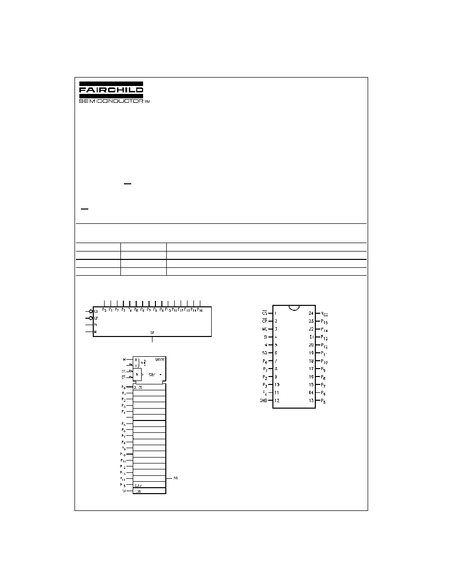
16-Bit Serial/Parallel-In, Serial-Out Shift Register
General Description
The 74F676 contains 16 flip-flops with provision for syn-
chronous parallel or serial entry and serial output. When
the Mode (M) input is HIGH, information present on the
parallel data (P
0
≠P
15
) inputs is entered on the falling edge
of the Clock Pulse (CP) input signal. When M is LOW, data
is shifted out of the most significant bit position while infor-
mation present on the Serial (SI) input shifts into the least
significant bit position. A HIGH signal on the Chip Select
(CS) input prevents both parallel and serial operations.
Features
s
16-bit parallel-to-serial conversion
s
16-bit serial-in, serial-out
s
Chip select control
s
Slim 24 lead 300 mil package
Ordering Code:
Devices also available in Tape and Reel. Specify by appending the suffix letter "X" to the ordering code.
Logic Symbols
IEEE/IEC
Connection Diagram
Order Number
Package Number
Package Description
74F676SC
M24B
28-Lead Small Outline Integrated Circuit (SOIC), JEDEC MS-013, 0.300 Wide
74F676PC
N24A
24-Lead Plastic Dual-In-Line Package (PDIP), JEDEC MS-010, 0.600 Wide
74F676SPC
N24C
24-Lead Plastic Dual-In-Line Package (PDIP), JEDEC MS-100, 0.300 Wide
www.fairchildsemi.com
2
74F676
Unit Loading/Fan Out
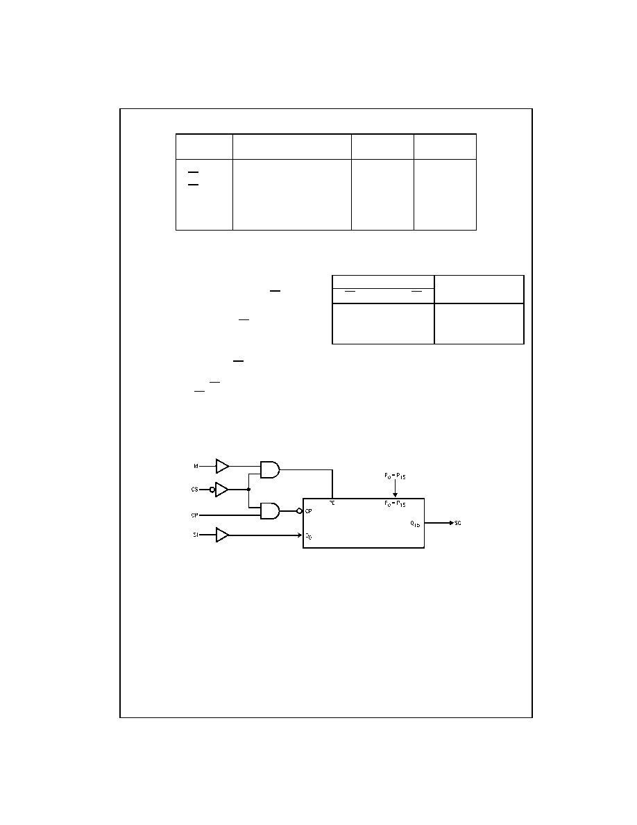
Functional Description
The 16-bit shift register operates in one of three modes, as
indicated in the Shift Register Operations Table.
HOLD-- a HIGH signal on the Chip Select (CS) input pre-
vents clocking, and data is stored in the sixteen registers.
Shift/Serial Load-- data present on the SI pin shifts into
the register on the falling edge of CP. Data enters the Q
0
position and shifts toward Q
15
on successive clocks, finally
appearing on the SO pin.
Parallel Load-- data present on P
0
≠P
15
are entered into
the register on the falling edge of CP. The SO output repre-
sents the Q
15
register output.
To prevent false clocking, CP must be LOW during a LOW-
to-HIGH transition of CS.
Shift Register Operations Table
H
=
HIGH Voltage Level
L
=
LOW Voltage Level
X
=
Immaterial
=
HIGH-to-LOW Transition
Block Diagram
Pin Names
Description
U.L.
Input I
IH
/I
IL
HIGH/LOW
Output I
OH
/I
OL
P
0
≠P
15
Parallel Data Inputs
1.0/1.0
20
µ
A/
-
0.6 mA
CS
Chip Select Input (Active LOW)
1.0/1.0
20
µ
A/
-
0.6 mA
CP
Clock Pulse Input (Active LOW)
1.0/1.0
20
µ
A/
-
0.6 mA
M
Mode Select Input
1.0/1.0
20
µ
A/
-
0.6 mA
SI
Serial Data Input
1.0/1.0
20
µ
A/
-
0.6 mA
SO
Serial Output
50/33.3
-
1 mA/20 mA
Control Input
Operating Mode
CS
M
CP
H
X
X
Hold
L
L
Shift/Serial Load
L
H
Parallel Load

3
www.fairchildsemi.com
7
4F676
Absolute Maximum Ratings
(Note 1)
Recommended Operating
Conditions
Note 1: Absolute maximum ratings are values beyond which the device
may be damaged or have its useful life impaired. Functional operation
under these conditions is not implied.
Note 2: Either voltage limit or current limit is sufficient to protect inputs.
DC Electrical Characteristics
Storage Temperature
-
65
∞
C to
+
150
∞
C
Ambient Temperature under Bias
-
55
∞
C to
+
125
∞
C
Junction Temperature under Bias
-
55
∞
C to
+
150
∞
C
V
CC
Pin Potential to Ground Pin
-
0.5V to
+
7.0V
Input Voltage (Note 2)
-
0.5V to
+
7.0V
Input Current (Note 2)
-
30 mA to
+
5.0 mA
Voltage Applied to Output
in HIGH State (with V
CC
=
0V)
Standard Output
-
0.5V to V
CC
3-STATE Output
-
0.5V to
+
5.5V
Current Applied to Output
in LOW State (Max)
twice the rated I
OL
(mA)
Free Air Ambient Temperature
0
∞
C to
+
70
∞
C
Supply Voltage
+
4.5V to
+
5.5V
Symbol
Parameter
Min
Typ
Max
Units
V
CC
Conditions
V
IH
Input HIGH Voltage
2.0
V
Recognized as a HIGH Signal
V
IL
Input LOW Voltage
0.8
V
Recognized as a LOW Signal
V
CD
Input Clamp Diode Voltage
-
1.2
V
Min
I
IN
=
-
18 mA
V
OH
Output HIGH
10% V
CC
2.5
V
Min
I
OH
=
-
1 mA
Voltage
5% V
CC
2.7
I
OH
=
-
1 mA
V
OL
Output LOW
10% V
CC
0.5
V
Min
I
OL
=
20 mA
Voltage
I
IH
Input HIGH
5.0
µ
A
Max
V
IN
=
2.7V
Current
I
BVI
Input HIGH Current
7.0
µ
A
Max
V
IN
=
7.0V
Breakdown Test
I
CEX
Output HIGH
50
µ
A
Max
V
OUT
=
V
CC
Leakage Current
V
ID
Input Leakage
4.75
V
0.0
I
ID
=
1.9
µ
A,
Test
All Other Pins Grounded
I
OD
Output Leakage
3.75
µ
A
0.0
V
IOD
=
150 mV,
Circuit Current
All Other Pins Grounded
I
IL
Input LOW Current
-
0.6
mA
Max
V
IN
=
0.5V
I
OS
Output Short-Circuit Current
-
60
-
150
mA
Max
V
OUT
=
0V
I
CC
Power Supply Current
72
mA
Max

www.fairchildsemi.com
4
74F676
AC Electrical Characteristics
AC Operating Requirements
Symbol
Parameter
T
A
=
+
25
∞
C
T
A
=
-
55
∞
C to 125
∞
C
T
A
=
0
∞
C to
+
70
∞
C
Units
V
CC
=
+
5.0V
V
CC
=
+
5.0V
V
CC
=
+
5.0V
C
L
=
50 pF
C
L
=
50 pF
C
L
=
50 pF
Min
Typ
Max
Min
Max
Min
Max
f
MAX
Maximum Clock Frequency
100
110
45
90
MHz
t
PLH
Propagation Delay
4.5
9.0
11.0
4.5
17.0
4.5
12.0
ns
t
PHL
CP to SO
5.0
9.0
12.5
5.0
14.5
5.0
13.5
Symbol
Parameter
T
A
=
+
25
∞
C
T
A
=
-
55
∞
C to 125
∞
C
T
A
, V
CC
=
____
Units
V
CC
=
+
5.0V
V
CC
=
+
5.0V
V
CC
=
+
5.0V
Min
Max
Min
Max
Min
Max
t
S
(H)
Setup Time, HIGH or LOW
4.0
4.0
4.0
t
S
(L)
SI to CP
4.0
4.0
4.0
ns
t
H
(H)
Hold Time, HIGH or LOW
4.0
4.0
4.0
t
H
(L)
SI to CP
4.0
4.0
4.0
t
S
(H)
Setup Time, HIGH or LOW
3.0
3.0
3.0
t
S
(L)
P
n
to CP
3.0
3.0
3.0
ns
t
H
(H)
Hold Time, HIGH or LOW
4.0
4.0
4.0
t
H
(L)
P
n
to CP
4.0
4.0
4.0
t
S
(H)
Setup Time, HIGH or LOW
8.0
8.0
8.0
t
S
(L)
M to CP
8.0
8.0
8.0
ns
t
H
(H)
Hold Time, HIGH or LOW
2.0
2.0
2.0
t
H
(L)
M to CP
2.0
2.0
2.0
t
S
(L)
Setup Time, LOW
10.0
12.0
10.0
CS to CP
ns
t
H
(H)
Hold Time, HIGH
10.0
10.0
10.0
CS to CP
t
W
(H)
CP Pulse Width
4.0
5.0
4.0
ns
t
W
(L)
HIGH or LOW
6.0
9.0
6.0
5
www.fairchildsemi.com
7
4F676
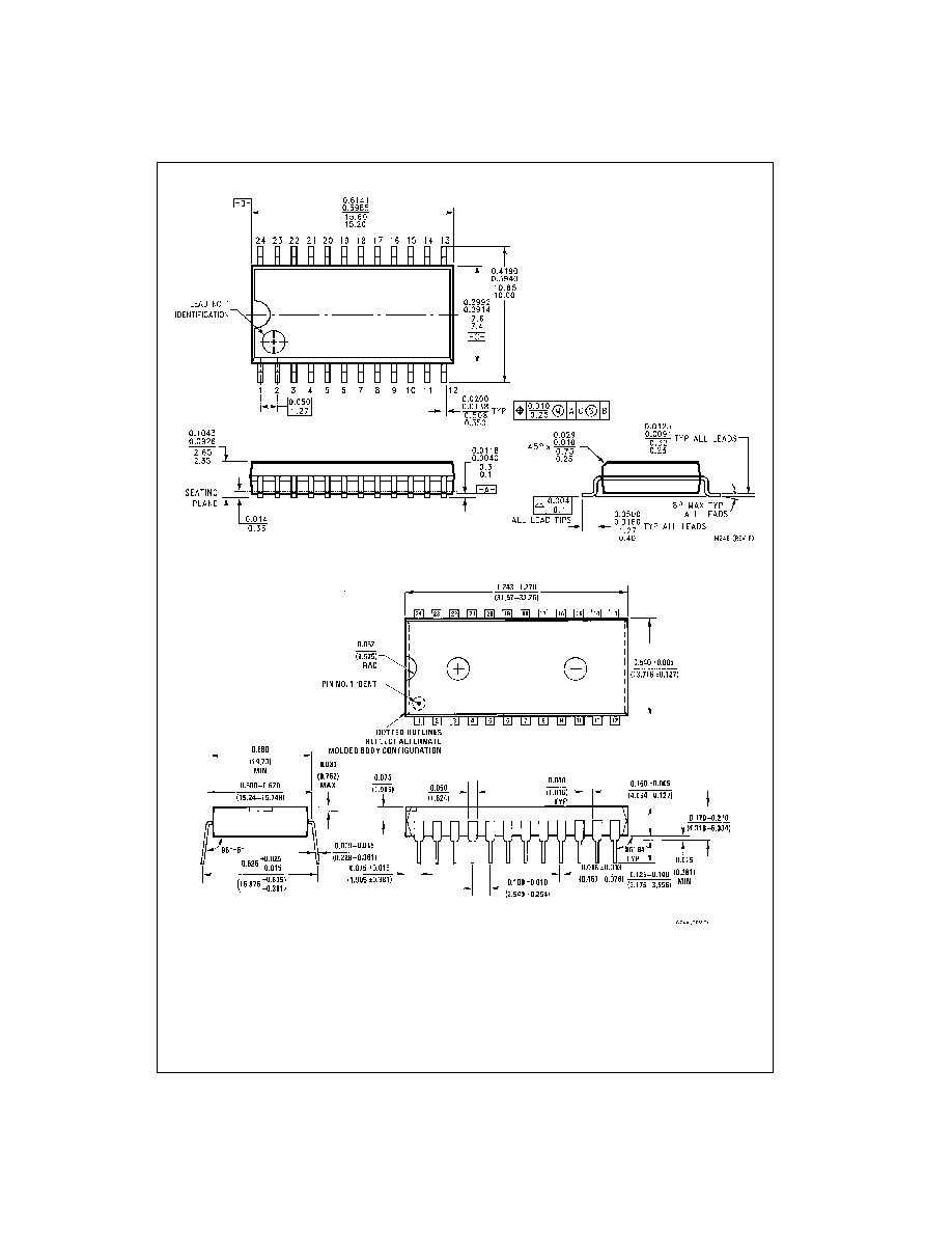
Physical Dimensions
inches (millimeters) unless otherwise noted
28-Lead Small Outline Integrated Circuit (SOIC), JEDEC MS-013, 0.300 Wide
Package Number M24B
24-Lead Plastic Dual-In-Line Package (PDIP), JEDEC MS-010, 0.600 Wide
Package Number N24A