 | –≠–ª–µ–∫—Ç—Ä–æ–Ω–Ω—ã–π –∫–æ–º–ø–æ–Ω–µ–Ω—Ç: 74F74PC | –°–∫–∞—á–∞—Ç—å:  PDF PDF  ZIP ZIP |
© 2000 Fairchild Semiconductor Corporation
DS009469
www.fairchildsemi.com
April 1988
Revised September 2000
7
4
F74
Dual
D
-
T
y
pe Posit
i
ve Edge-
T
ri
ggered Fl
ip-
F
lop
74F74
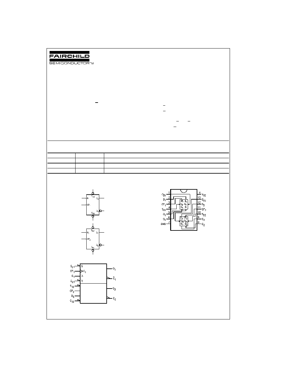
Dual D-Type Positive Edge-Triggered Flip-Flop
General Description
The F74 is a dual D-type flip-flop with Direct Clear and Set
inputs and complementary (Q, Q) outputs. Information at
the input is transferred to the outputs on the positive edge
of the clock pulse. Clock triggering occurs at a voltage level
of the clock pulse and is not directly related to the transition
time of the positive-going pulse. After the Clock Pulse input
threshold voltage has been passed, the Data input is
locked out and information present will not be transferred to
the outputs until the next rising edge of the Clock Pulse
input.
Asynchronous Inputs:
LOW input to S
D
sets Q to HIGH level
LOW input to C
D
sets Q to LOW level
Clear and Set are independent of clock
Simultaneous LOW on C
D
and S
D
makes both Q and Q HIGH
Ordering Code:
Devices also available in Tape and Reel. Specify by appending the suffix letter "X" to the ordering code.
Logic Symbols
IEEE/IEC
Connection Diagram
Order Number
Package Number
Package Description
74F74SC
M14A
14-Lead Small Outline Integrated Circuit (SOIC), JEDEC MS-120, 0.150 Narrow
74F74SJ
M14D
14-Lead Small Outline Package (SOP), EIAJ TYPE II, 5.3mm Wide
74F74PC
N14A
14-Lead Plastic Dual-In-Line Package (PDIP), JEDEC MS-001, 0.300 Wide
www.fairchildsemi.com
2
74F74
Unit Loading/Fan Out
Truth Table
H (h)
=
HIGH Voltage Level
L (l)
=
LOW Voltage Level
X
=
Immaterial
Q
0
=
Previous Q (Q) before LOW-to-HIGH Clock Transition
Lower case letters indicate the state of the referenced input or output one setup time prior to the LOW-to-HIGH clock transition.
Logic Diagram
Please note that this diagram is provided only for the understanding of logic operations and should not be used to estimate propagation delays.
Pin Names
Description
U.L.
Input I
IH
/I
IL
HIGH/LOW
Output I
OH
/I
OL
D
1
, D
2
Data Inputs
1.0/1.0
20
µ
A/
-
0.6 mA
CP
1
, CP
2
Clock Pulse Inputs (Active Rising Edge)
1.0/1.0
20
µ
A/
-
0.6 mA
C
D1
, C
D2
Direct Clear Inputs (Active LOW)
1.0/3.0
20
µ
A/
-
1.8 mA
S
D1
, S
D2
Direct Set Inputs (Active LOW)
1.0/3.0
20
µ
A/
-
1.8 mA
Q
1
, Q
1
, Q
2
, Q
2
Outputs
50/33.3
-
1 mA/20 mA
Inputs
Outputs
S
D
C
D
CP
D
Q
Q
L
H
X
X
H
L
H
L
X
X
L
H
L
L
X
X
H
H
H
H
h
H
L
H
H
l
L
H
H
H
L
X
Q
0
Q
0
3
www.fairchildsemi.com
74
F
7
4
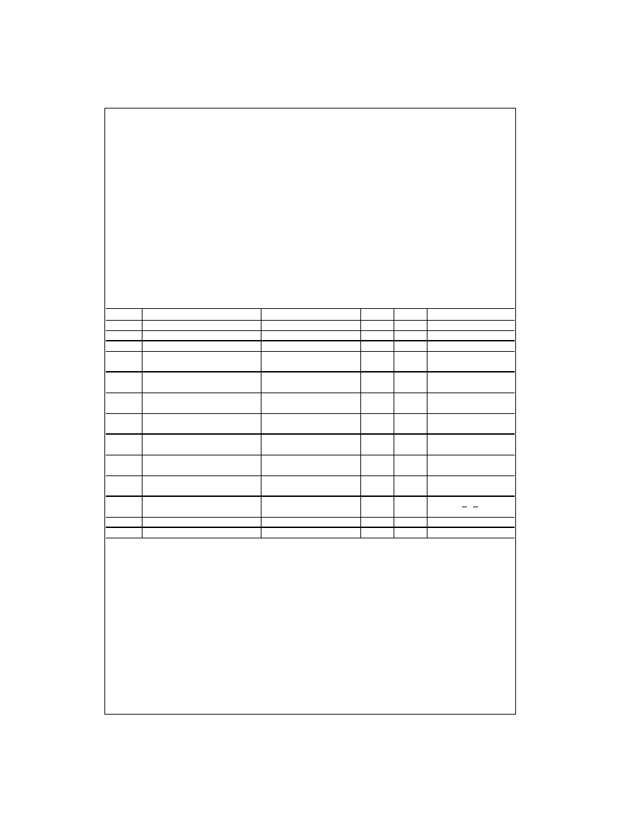
Absolute Maximum Ratings
(Note 1)
Recommended Operating
Conditions
Note 1: Absolute maximum ratings are values beyond which the device
may be damaged or have its useful life impaired. Functional operation
under these conditions is not implied.
Note 2: Either voltage limit or current limit is sufficient to protect inputs.
DC Electrical Characteristics
Storage Temperature
-
65
∞
C to
+
150
∞
C
Ambient Temperature under Bias
-
55
∞
C to
+
125
∞
C
Junction Temperature under Bias
-
55
∞
C to
+
150
∞
C
V
CC
Pin Potential to Ground Pin
-
0.5V to
+
7.0V
Input Voltage (Note 2)
-
0.5V to
+
7.0V
Input Current (Note 2)
-
30 mA to
+
5.0 mA
Voltage Applied to Output
in HIGH State (with V
CC
=
0V)
Standard Output
-
0.5V to V
CC
3-STATE Output
-
0.5V to
+
5.5V
Current Applied to Output
in LOW State (Max)
twice the rated I
OL
(mA)
ESD Last Passing Voltage (Min)
4000V
Free Air Ambient Temperature
0
∞
C to
+
70
∞
C
Supply Voltage
+
4.5V to
+
5.5V
Symbol
Parameter
Min
Typ
Max
Units
V
CC
Conditions
V
IH
Input HIGH Voltage
2.0
V
Recognized as a HIGH Signal
V
IL
Input LOW Voltage
0.8
V
Recognized as a LOW Signal
V
CD
Input Clamp Diode Voltage
-
1.2
V
Min
I
IN
=
-
18 mA
V
OH
Output HIGH
10% V
CC
2.5
V
Min
I
OH
=
-
1 mA
Voltage
5% V
CC
2.7
I
OH
=
-
1 mA
V
OL
Output LOW
10% V
CC
0.5
V
Min
I
OL
=
20 mA
Voltage
I
IH
Input HIGH
5.0
µ
A
Max
V
IN
=
2.7V
Current
I
BVI
Input HIGH Current
7.0
µ
A
Max
V
IN
=
7.0V
Breakdown Test
I
CEX
Output HIGH
50
µ
A
Max
V
OUT
=
V
CC
Leakage Current
V
ID
Input Leakage
4.75
V
0.0
I
ID
=
1.9
µ
A
Test
All Other Pins Grounded
I
OD
Output Leakage
3.75
µ
A
0.0
V
IOD
=
150 mV
Circuit Current
All Other Pins Grounded
I
IL
Input LOW Current
-
0.6
mA
Max
V
IN
=
0.5V (D, CP)
-
1.8
V
IN
=
0.5V (C
D
, S
D
)
I
OS
Output Short-Circuit Current
-
60
-
150
mA
Max
V
OUT
=
0V
I
CC
Power Supply Current
10.5
16.0
mA
Max
www.fairchildsemi.com
4
74F74
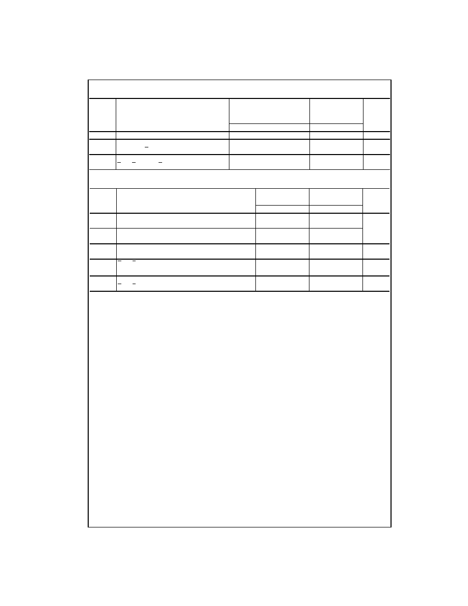
AC Electrical Characteristics
AC Operating Requirements
Symbol
Parameter
T
A
=
+
25
∞
C
T
A
=
0
∞
C to
+
70
∞
C
Units
V
CC
=
+
5.0V
V
CC
=
+
5.0V
C
L
=
50 pF
C
L
=
50 pF
Min
Typ
Max
Min
Max
f
MAX
Maximum Clock Frequency
100
125
100
MHz
t
PLH
Propagation Delay
3.8
5.3
6.8
3.8
7.8
ns
t
PHL
CP
n
to Q
n
or Q
n
4.4
6.2
8.0
4.4
9.2
t
PLH
Propagation Delay
3.2
4.6
6.1
3.2
7.1
ns
t
PHL
C
Dn
or S
Dn
to Q
n
or Q
n
3.5
7.0
9.0
3.5
10.5
Symbol
Parameter
T
A
=
+
25
∞
C
T
A
=
0
∞
C to
+
70
∞
C
Units
V
CC
=
+
5.0V
V
CC
=
+
5.0V
Min
Max
Min
Max
t
S
(H)
Setup Time, HIGH or LOW
2.0
2.0
ns
t
S
(L)
D
n
to CP
n
3.0
3.0
t
H
(H)
Hold Time, HIGH or LOW
1.0
1.0
t
H
(L)
D
n
to CP
n
1.0
1.0
t
W
(H)
CP
n
Pulse Width
4.0
4.0
ns
t
W
(L)
HIGH or LOW
5.0
5.0
t
W
(L)
C
Dn
or S
Dn
Pulse Width
4.0
4.0
ns
LOW
t
REC
Recovery Time
2.0
2.0
ns
C
Dn
or S
Dn
to CP
5
www.fairchildsemi.com
74
F
7
4
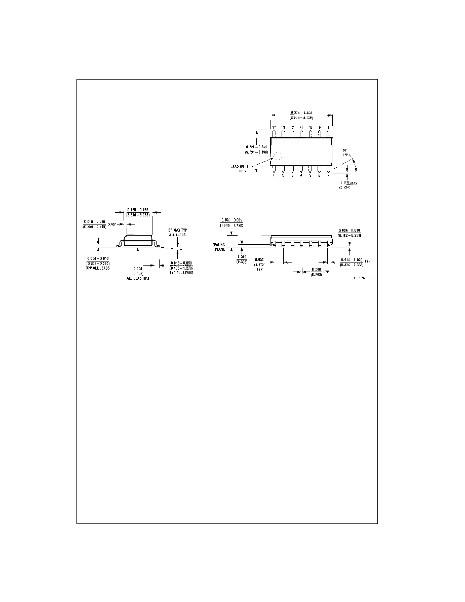
Physical Dimensions
inches (millimeters) unless otherwise noted
14-Lead Small Outline Integrated Circuit (SOIC), JEDEC MS-120, 0.150 Narrow
Package Number M14A