© 1999 Fairchild Semiconductor Corporation
DS010990
www.fairchildsemi.com
May 1992
Revised August 1999
7
4FR900 9
-
Bit
,
3-
Port
Lat
chabl
e Dat
apat
h Mult
i
p
lexer
74FR900
9-Bit, 3-Port Latchable Datapath Multiplexer
General Description
The 74FR900 is a data bus multiplexer routing any of three
9-bit ports to any other one of the three ports. Readback of
data latched from any port onto itself is also possible. The
74FR900 maintains separate control of all latch-enable,
output enable and select inputs for maximum flexibility.
PINV allows inversion of the data from the C
8
to A
8
or B
8
path. This is useful for control of the parity bit in systems
diagnostics.
Fairchild's 74FR25900 includes 25
resistors in series with
port A and B outputs. Resistors minimize undershoot and
ringing which may damage or corrupt sensitive device
inputs driven by these ports.
Features
s
9-bit data ports for systems carrying parity bits
s
Readback capability for system self checks.
s
Independent control lines for maximum flexibility
s
Guaranteed multiple output switching and 250 pF load
delays
s
Outputs optimized for dynamic bus drive capability
s
PINV parity control facilitates system diagnostics
s
FR25900 resistor option for driving MOS inputs such as
DRAM arrays
Ordering Code:
Devices also available in Tape and Reel. Specify by appending the suffix letter "X" to the ordering code.
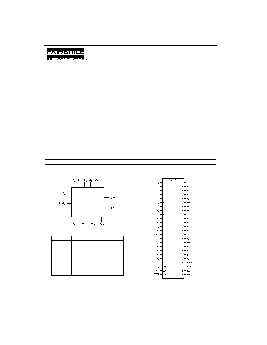
Logic Symbol
Pin Description
Connection Diagram
Order Number
Package Number
Package Description
74FR900SSC
MS48A
48-Lead Small Shrink Outline Package (SSOP), JEDEC MO-118, 0.300 Wide
Pin Names
Description
LExx
Latch Enable Inputs
OE
x
Output Enable Inputs
PINV
Parity Invert Input
S
0
, S
1
Select Inputs
A
0
≠A
8
Port A Inputs or 3-STATE Outputs
B
0
≠B
8
Port B Inputs or 3-STATE Outputs
C
0
≠C
8
Port C Inputs or 3-STATE Outputs
www.fairchildsemi.com
2
74FR900
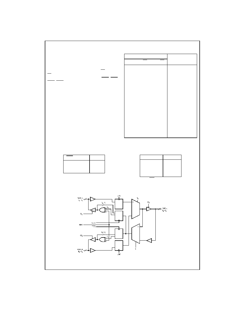
Functional Description
The 74FR900 allows 9-bit data to be transferred from any
of three 9-bit I/O ports to either of the two remaining I/O
ports. The device employs latches in all paths for either
transparent or synchronous operation. Readback capability
from any port to itself is also possible.
Data transfer within the 74FR900 is controlled through use
of the select (S
0
and S
1
) and output-enable (OE
A
, OE
B
and
OE
C
) inputs as described in Table 1. Additional control is
available by use of the latch-enable inputs (LEAC, LECA,
LEBC, LECB) allowing either synchronous or transparent
transfers (see Table 2). Table 1 indicates several readback
conditions. By latching data on a given port and initiating
the readback control configuration, previous data may be
read for system verification or diagnostics. This mode may
be useful in implementing system diagnostics.
Data at the port to be readback must be latched prior to
enabling the outputs on that port. If this is not done, a
closed data loop will result causing possible data integrity
problems. Note that the A and B ports allow readback with-
out affecting any other port. Port C, however, requires inter-
ruption of either port A or B to complete its readback path.
PINV controls inversion of the C
8
bit. A low on PINV allows
C
8
data to pass unaltered. A high causes inversion of the
data. See Table 3. This feature allows forcing of parity
errors for use in system diagnostics. This is particularly
helpful in 486 processor designs as the 486 does not pro-
vide odd/even parity selection internally.
TABLE 1. Datapath Control
Note 1: Readback operation in latched mode only. Transparent operation
could result in unpredictable results.
TABLE 2. Latch-Enable Control
TABLE 3. PINV Control
L
=
LOW Voltage
H
=
HIGH Voltage Level
Q
0
=
Output state prior to LExx LOW-to-HIGH transition
Logic Diagram
Inputs
Function
S
0
S
1
OE
A
OE
B
OE
C
L
X
H
L
L
Port A to Port C
L
L
H
H
H
Port A to Port B
L
O
H
H
L
Port A to B
+
C
H
L
L
L
H
Port B to Port A
H
X
H
L
L
Port B to Port C
H
O
L
L
L
Port B to A
+
C
X
H
L
L
H
Port C to Port A
X
H
H
H
H
Port C to Port B
X
H
L
H
H
Port C to A
+
B
X
X
H
L
H
Outputs Disabled
L
L
L
X
X
(Readback to A)
(Note 1)
L
H
L
X
L
(Readback to A or C)
(Note 1)
H
L
X
H
X
(Readback to B)
(Note 1)
H
H
X
H
L
(Readback to B or C)
(Note 1)
LExx
Input
Output
L
L
L
L
H
H
H
X
Q
0
PINV
C
8
A
8
or B
8
L
L
L
L
H
H
H
L
H
H
H
L
3
www.fairchildsemi.com
7
4FR900
Absolute Maximum Ratings
(Note 2)
Recommended Operating
Conditions
Note 2: Absolute maximum ratings are values beyond which the device
may be damaged or have its useful life impaired. Functional operation
under these conditions is not implied.
Note 3: Either voltage limit or current limit is sufficient to protect inputs.
DC Electrical Characteristics
Note 4: 2 ports active only
Storage Temperature
-
65
∞
C to
+
150
∞
C
Ambient Temperature under Bias
-
55
∞
C to
+
125
∞
C
Junction Temperature under Bias
-
55
∞
C to
+
150
∞
C
V
CC
Pin Potential to Ground Pin
-
0.5V to
+
7.0V
Input Voltage (Note 3)
-
0.5V to
+
7.0V
Input Current (Note 3)
-
30 mA to
+
5.0 mA
Voltage Applied to Output
in HIGH State (with V
CC
=
0V)
Standard Output
-
0.5V to V
CC
3-STATE Output
-
0.5V to
+
5.5V
Current Applied to Output
in LOW State (Max)
twice the rated I
OL
(mA)
ESD Last Passing Voltage (Min)
4000V
Free Air Ambient Temperature
0
∞
C to
+
70
∞
C
Supply Voltage
+
4.5V to
+
5.5V
Symbol
Parameter
Min
Typ
Max
Units
V
CC
Conditions
V
IH
Input HIGH Voltage
2.0
V
Recognized HIGH Signal
V
IL
Input LOW Voltage
0.8
V
Recognized LOW Signal
V
CD
Input Clamp Diode Voltage
-
1.2
V
Min
I
IN
=
-
18 mA
V
OH
Output HIGH Voltage
2.4
V
Min
I
OH
=
-
3 mA (A
n
, B
n
, C
n
)
2.0
V
Min
I
OH
=
-
15 mA (A
n
, B
n
, C
n
)
V
OL
Output LOW Voltage
0.50
V
Min
I
OL
=
24 mA (A
n
, B
n
, C
n
)
I
IH
Input HIGH Current
5
µ
A
Max
V
IN
=
2.7V (Control Inputs)
I
BVI
Input HIGH Current
7
µ
A
Max
V
IN
=
7.0V (Control Inputs)
Breakdown Test
I
BVIT
Input HIGH Current
100
µ
A
Max
V
IN
=
5.5V (A
n
, B
n
, C
n
)
Breakdown Test (I/O)
I
IL
Input LOW Current
-
150
µ
A
Max
V
IN
=
0.5V (Control Inputs)
V
ID
Input Leakage Test
4.75
V
0.0
I
ID
=
1.9
µ
A,
All Other Pins Grounded
I
OD
Output Circuit Leakage Test
3.75
V
0.0
V
IOD
=
150 mV,
All Other Pins Grounded
I
IH
+
I
OZH
Output Leakage Current
25
µ
A
Max
V
OUT
=
2.7V (A
n
, B
n
, C
n
)
I
IIL
+
I
OZL
Output Leakage Current
-
150
µ
A
Max
V
OUT
=
0.5V (A
n
, B
n
, C
n
)
I
OS
Output Short Circuit Current
-
100
-
225
mA
Max
V
OUT
=
0.0V (A
n
, B
n
, C
n
)
I
CEX
Output HIGH Leakage Current
50
µ
A
Max
V
OUT
=
V
CC
(A
n
, B
n
, C
n
)
I
ZZ
Bus Drainage Test
100
µ
A
0.0
V
OUT
=
5.25V (A
n
, B
n
, C
n
)
I
CCH
Power Supply Current
115
150
mA
Max
All Outputs HIGH (Note 4)
I
CCL
Power Supply Current
170
200
mA
Max
All Outputs LOW (Note 4)
I
CCZ
Power Supply Current
147
175
mA
Max
Outputs in 3-STATE

www.fairchildsemi.com
4
74FR900
AC Electrical Characteristics
AC Operating Requirements
Extended AC Electrical Characteristics
Symbol
Parameter
T
A
=
+
25
∞
C
T
A
=
0
∞
C to
+
70
∞
C
Units
V
CC
=
+
5.0V
V
CC
=
+
5.0V
C
L
=
50 pF
C
L
=
50 pF
Min
Typ
Max
Min
Max
t
PLH
Propagation Delay
t
PHL
A
n
or B
n
to C
n
2.0
4.2
7.0
2.0
7.0
ns
C
n
to A
n
or B
n
t
PLH
Propagation Delay
2.5
4.8
7.5
2.5
7.5
ns
t
PHL
C
8
to A
8
or B
8
(PINV HIGH)
t
PLH
Propagation Delay
4.5
6.4
10.0
4.5
10.0
ns
t
PHL
A
n
to B
n
, B
n
to A
n
t
PLH
Propagation Delay
4.5
6.8
10.0
4.5
10.0
ns
t
PHL
LEAC to C
n
, LEBC to C
n
t
PLH
Propagation Delay
3.0
6.0
9.5
3.0
9.5
ns
t
PHL
LECA to A
n
, LECB to B
n
t
PLH
Propagation Delay
3.0
6.0
10.0
3.0
10.0
ns
t
PHL
S
0
to C
n
t
PLH
Propagation Delay
3.5
6.5
11.0
3.5
11.0
ns
t
PHL
S
1
to A
n
or B
n
t
PLH
Propagation Delay
2.0
5.0
9.0
2.0
9.0
ns
t
PHL
PINV to A
8
or B
8
t
PZH
Output Enable Time
2.0
4.0
6.5
2.0
6.5
ns
t
PZL
A
n
, C
n
t
PHZ
Output Disable Time
1.5
4.0
6.0
1.5
6.0
ns
t
PLZ
A
n
, C
n
t
PZH
Output Enable Time
2.0
5.0
7.0
2.0
7.0
ns
t
PZL
B
n
t
PHZ
Output Disable Time
2.0
5.0
7.0
2.0
7.0
ns
t
PLZ
B
n
Symbol
Parameter
T
A
=
+
25
∞
C
T
A
=
0
∞
C to
+
70
∞
C
Units
V
CC
=
+
5.0V
V
CC
=
+
5.0V
C
L
=
50 pF
C
L
=
50 pF
Min
Typ
Max
Min
Max
t
S
(H)
Setup Time, HIGH or LOW
4.0
2.0
4.0
ns
t
S
(L)
A
n
to LEAC, B
n
to LEBC
t
H
(H)
Hold Time, HIGH or LOW
1.0
-
2.0
1.0
ns
t
H
(L)
A
n
to LEAC, B
n
to LEBC
t
S
(H)
Setup Time, HIGH or LOW
3.0
1.0
3.0
ns
t
S
(L)
C
n
to LECA or LECB
t
H
(H)
Hold Time, HIGH or LOW
1.0
-
1.0
1.0
ns
t
H
(L)
C
n
to LECA or LECB
t
W
(H)
LE Pulse Width LOW
8.0
4.0
8.0
ns
Symbol
Parameter
T
A
=
0
∞
C to
+
70
∞
C
T
A
=
0
∞
C to
+
70
∞
C
Units
V
CC
=
+
5.0V
V
CC
=
+
5.0V
C
L
=
50 pF
C
L
=
250 pF
Nine Outputs Switching
(Note 6)
(Note 5)
Min
Max
Min
Max
t
PLH
Propagation Delay

5
www.fairchildsemi.com
7
4FR900
Extended AC Electrical Characteristics
(Continued)
Note 5: This specification is guaranteed but not tested. The limits apply to propagation delays for all paths described switching in phase,
i.e., all LOW-to-HIGH, HIGH-to-LOW, 3-STATE-to-HIGH, etc.
Note 6: This specification is guaranteed but not tested. The limits represent propagation delays with 250 pF load capacitors in place of the 50 pF load capac-
itors standard AC load. This specification pertains to single output switching only.
Symbol
Parameter
T
A
=
0
∞
C to
+
70
∞
C
T
A
=
0
∞
C to
+
70
∞
C
Units
V
CC
=
+
5.0V
V
CC
=
+
5.0V
C
L
=
50 pF
C
L
=
250 pF
Nine Outputs Switching
(Note 6)
(Note 5)
Min
Max
Min
Max
t
PHL
A
n
or B
n
to C
n
2.0
9.0
2.5
10.5
ns
C
n
to A
n
or B
n
t
PLH
Propagation Delay
3.5
11.0
ns
t
PHL
C
8
to A
8
or B
8
(PINV HIGH)
t
PLH
Propagation Delay
4.5
12.0
5.5
13.5
ns
t
PHL
A
n
to B
n
, B
n
to A
n
t
PLH
Propagation Delay
4.5
12.0
5.5
13.5
ns
t
PHL
LEAC to C
n
, LEBC to C
n
t
PLH
Propagation Delay
3.0
11.5
4.0
13.5
ns
t
PHL
LECA to A
n
, LECB to B
n
t
PLH
Propagation Delay
3.0
11.0
3.0
14.0
ns
t
PHL
S
0
to C
n
t
PLH
Propagation Delay
3.5
12.0
4.5
15.0
ns
t
PHL
S
1
to A
n
or B
n
t
PLH
Propagation Delay
2.5
12.0
ns
t
PHL
PINV to A
8
or B
8
t
PZH
Output Enable Time
2.0
8.0
ns
t
PZL
A
n
, C
n
t
PHZ
Output Disable Time
1.5
6.0
ns
t
PLZ
A
n
, C
n
t
PZH
Output Enable Time
2.0
8.0
ns
t
PZL
B
n
t
PHZ
Output Disable Time
2.0
7.0
ns
t
PLZ
B
n